 ChipApex | Global Electronic Components Supplier
SEARCH
Search Product
Search Post
— IC芯片 | 连接器 | 传感器 | 被动器件 —
Search productSearch post
— IC芯片 | 连接器 | 传感器 | 被动器件 —
Consult the customer manager about the wholesale price.
consultation hotline:86-132-6715-2157
email:[email protected]
Contact the product manager for consultation. One-stop consultation is available.
Do you want a lower wholesale price? Please send us your inquiry and we will reply immediately.
The UCC5672PWP is a multi-mode SCSI terminator manufactured by Texas Instruments in a 28-pin TSSOP package. It supports operation within a supply voltage range of 2.7V to 5.25V and functions across a commercial temperature range of 0°C to 70°C. The device integrates both single-ended (SE) and low-voltage differential (LVD) termination networks for 9-line SCSI buses. Electrical specifications include a typical LVD mode supply current of 23mA, an SE mode current of 14mA, and a differential impedance of 105Ω. It features built-in SPI-3 mode change filtering with a delay of up to 300ms.
Verify the specific ordering suffix against the manufacturer's official documentation to confirm packaging details. The PWP suffix indicates a tube carrier format containing 50 units per tube. Confirm that the component status remains active for production use before finalizing procurement plans.
Select this component for designs requiring a monolithic solution for 9-line SCSI termination. Ensure the system power supply falls within the 2.7V to 5.25V operating range. Verify that the PCB layout accommodates the thermal requirements of the TSSOP-28 package, specifically connecting the HS/GND pins to ground planes.
This part belongs to the UCC5672 family of multi-mode terminators. It serves as a transition component allowing coexistence of legacy Single Ended devices and modern Low Voltage Differential devices on the same SCSI bus architecture without manual configuration.
The UCC5672MWP is a compatible alternative offered in a 36-pin QSOP package. Verify pinout compatibility and physical footprint constraints before substituting the PWP variant with the MWP variant.
The device monitors the voltage on the DIFSENS pin. If the voltage is below 0.5V, it activates Single Ended mode. Between 0.7V and 1.9V, it switches to LVD SCSI mode. Above 2.4V, it enters a high-impedance state for High Voltage Differential buses.
The DIFFB pin receives the filtered DIFSENS signal through a 50Hz noise filter. It provides the input to the internal comparators that decide which termination network to activate.
The HS/GND pins must be connected to large ground area traces or multiple vias to the ground plane. This connection is critical for conducting heat away from the die to maintain safe junction temperatures.
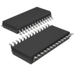 UCC5672PWP
The activity of extra discounts on wholesale prices is in full swing…
Please fill in your contact information and we will send you the latest wholesale price list.





