 ChipApex | Global Electronic Components Supplier
SEARCH
Search Product
Search Post
— IC芯片 | 连接器 | 传感器 | 被动器件 —
Search productSearch post
— IC芯片 | 连接器 | 传感器 | 被动器件 —
Consult the customer manager about the wholesale price.
consultation hotline:86-132-6715-2157
email:[email protected]
Contact the product manager for consultation. One-stop consultation is available.
Do you want a lower wholesale price? Please send us your inquiry and we will reply immediately.
The UDA1345TS is a stereo audio CODEC integrating an ADC and DAC with bitstream conversion. It operates on a 2.4 V to 3.6 V supply, consuming 64 mW in record/playback mode. The device supports sampling frequencies from 8 kHz to 100 kHz using system clocks of 256fs, 384fs, or 512fs. It features a signal-to-noise ratio of up to 96 dB for the ADC and 100 dB for the DAC at 44.1 kHz. Digital interfaces include I2S-bus (up to 24 bits), MSB-justified (up to 20 bits), and LSB-justified formats (16, 18, 20 bits). Control is managed via L3 microcontroller interface or static pins.
Verify component authenticity through authorized NXP distributors or official channels. Confirm package integrity and pin alignment against SSOP28 specifications. Review datasheet revisions to ensure compatibility with current design requirements. Validate operating conditions against absolute maximum ratings prior to integration.
Select this component for applications requiring low-power stereo audio conversion with flexible digital interface options. Ensure system clock availability matches supported frequencies of 256fs, 384fs, or 512fs. Verify that the host controller supports the L3 interface protocol if dynamic configuration is required. Check voltage levels to ensure compatibility with the 2.4 V to 3.6 V supply range.
The UDA1345TS is part of NXP's economy audio CODEC family. It shares pin and function compatibility with the UDA1344TS and UDA1340M in L3 mode. The device utilizes bitstream conversion techniques to achieve high audio fidelity while maintaining low power consumption suitable for battery-operated devices.
UDA1344TS is confirmed as a pin and function compatible replacement in L3 microcontroller mode. Verify specific feature differences, such as the absence of bass-boost and treble controls in the UDA1345TS compared to other variants.
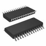 UDA1345TS/N2,112
The activity of extra discounts on wholesale prices is in full swing…
Please fill in your contact information and we will send you the latest wholesale price list.






