 ChipApex | Global Electronic Components Supplier
SEARCH
Search Product
Search Post
— IC芯片 | 连接器 | 传感器 | 被动器件 —
Search productSearch post
— IC芯片 | 连接器 | 传感器 | 被动器件 —
Consult the customer manager about the wholesale price.
consultation hotline:86-132-6715-2157
email:[email protected]
Contact the product manager for consultation. One-stop consultation is available.
Do you want a lower wholesale price? Please send us your inquiry and we will reply immediately.
The UJA1132HW/FD/3V/0Y is a system basis chip integrating a buck-boost converter, HS-CAN transceiver, and dual LIN transceivers. It operates within a supply voltage range of 2V to 28V and supports an operating temperature range of -40°C to 125°C (TA). The device features a current supply of 2.8mA and utilizes an HTQFP-48 (10x10) package. This component is designed for automotive applications requiring robust power management and multi-network communication capabilities.
Verify the specific suffix configuration against official NXP documentation, as variations exist in voltage and packaging options. Confirm end-of-life status or obsolescence through authorized distributors before procurement planning. Ensure compatibility with existing board layouts regarding the HTQFP-48 package dimensions and thermal requirements.
Select this component when a single IC solution is required to manage power conversion alongside both high-speed CAN and dual LIN communications. Consider the wide input voltage range and extended temperature specifications for harsh automotive environments. Evaluate the integration benefits against discrete solutions to reduce bill of materials and board space.
This part belongs to the UJA113x series of system basis chips from NXP Semiconductors. These devices are engineered to simplify automotive electronic design by combining essential power management and communication interfaces into a compact form factor, reducing complexity in vehicle network architectures.
Check for direct pin-to-pin compatible alternatives within the UJA113x family that may have updated lifecycle statuses. Verify functional equivalence regarding voltage ranges and protocol support if substituting with other manufacturers' system basis chips.
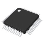 UJA1132HW/FD/3V/0Y
The activity of extra discounts on wholesale prices is in full swing…
Please fill in your contact information and we will send you the latest wholesale price list.





