ChipApex | Global Electronic Components Supplier
SEARCH
Search Product
Search Post
— IC芯片 | 连接器 | 传感器 | 被动器件 —
Search productSearch post
— IC芯片 | 连接器 | 传感器 | 被动器件 —
Consult the customer manager about the wholesale price.
consultation hotline:86-132-6715-2157
email:[email protected]
Contact the product manager for consultation. One-stop consultation is available.
Do you want a lower wholesale price? Please send us your inquiry and we will reply immediately.
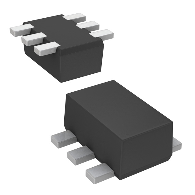
The Panasonic UP05C8B is a multi-chip discrete component integrating a silicon NPN epitaxial planar transistor and a CCD load device within a single SSMini6-F1 package. The transistor section provides a collector-base voltage of 30 V, collector-emitter voltage of 20 V, and a forward current transfer ratio (hFE) ranging from 65 to 160 at 1 mA. The integrated CCD load device features a limiting element voltage of 40 V and a pinch-off current between 3.5 mA and 5.5 mA at 10 V drain-source bias. Total power dissipation is rated at 125 mW.
Verify the specific lifecycle status on the manufacturer's official website before procurement, as this component may be subject to maintenance or discontinuation plans. Confirm that the SSMini6-F1 package dimensions and pinout align with existing board layouts. Ensure design margins respect the absolute maximum ratings for thermal and electrical stress.
Select this component when space constraints require combining an amplification stage with a constant current source for CCD sensors. It serves as a direct replacement for the 2SC3931 transistor paired with a separate CCD load device. Evaluate the transition frequency and noise figure requirements against the specified 640 MHz fT and 3.3 dB NF values.
This component belongs to the Multi Chip Discrete category, consolidating multiple functions into a single footprint. It replaces the traditional combination of a 2SC3931 transistor and a discrete CCD load device. The integration supports downsizing strategies in electronic equipment manufacturing by reducing the total number of required components.
The datasheet identifies the 2SC3931 transistor combined with a CCD load device as the basic part number equivalent. No other specific substitute part numbers are documented in the provided material.
The package contains six pins: Pin 1 is Emitter, Pin 2 is Base, Pin 3 is Gate, Pin 4 is Source, Pin 5 is Drain, and Pin 6 is Collector.
The transition frequency (fT) is 640 MHz under conditions of VCB = 6 V and IE = -1 mA at 200 MHz.
The maximum junction temperature (Tj) is 125 °C.
 UP05C8B00L
The activity of extra discounts on wholesale prices is in full swing…
Please fill in your contact information and we will send you the latest wholesale price list.