ChipApex | Global Electronic Components Supplier
SEARCH
Search Product
Search Post
— IC芯片 | 连接器 | 传感器 | 被动器件 —
Search productSearch post
— IC芯片 | 连接器 | 传感器 | 被动器件 —
Consult the customer manager about the wholesale price.
consultation hotline:86-132-6715-2157
email:[email protected]
Contact the product manager for consultation. One-stop consultation is available.
Do you want a lower wholesale price? Please send us your inquiry and we will reply immediately.
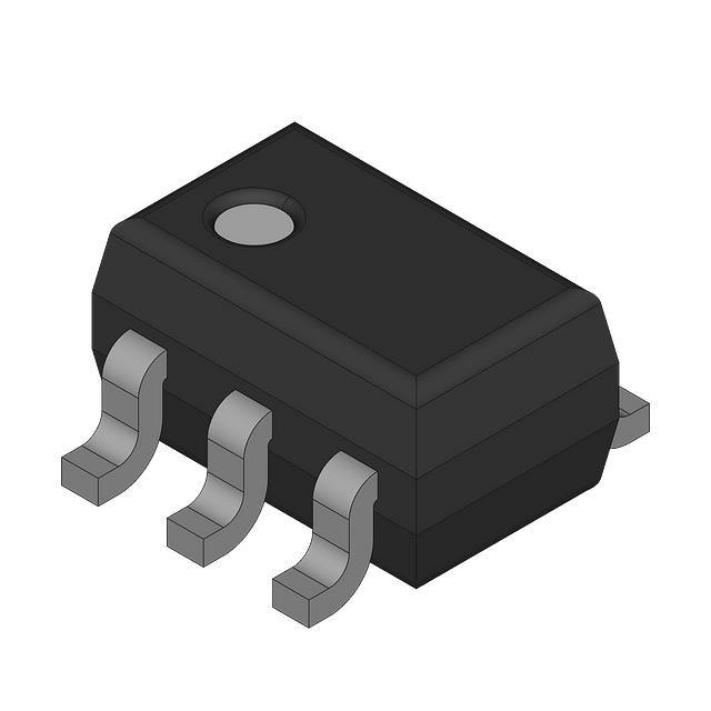
The V62/04735-01XE is a Mil Enhanced Single Bus Buffer Gate with 3-state output from the SN74LVC1G125-EP series. It operates within a supply voltage range of 1.65 V to 5.5 V and features one input line and one non-inverting output line. The device supports partial-power-down mode via Ioff circuitry, which disables outputs to prevent damaging current backflow when powered down. It provides an output drive of ±24 mA at 3.3 V and exhibits low power consumption with a maximum ICC of 10 μA. The component is housed in a SC70 (DCK) package.
Verify that the specific ordering suffix matches the required operating temperature range, as the base part number covers multiple variants. Confirm the DMS support status and pedigree documentation are included with the shipment. Ensure the component meets the specific qualification requirements for your application environment before final integration.
Select this component when extended temperature operation or military-grade reliability is required compared to standard catalog versions. Consider the SC70 package constraints for board space limitations. Evaluate the propagation delay characteristics against system timing requirements at the target supply voltage.
This part belongs to the SN74LVC1G125-EP family, representing the enhanced product version of the standard LVC logic buffer. It shares functional similarities with the CLVC1G125MDCKREP but includes specific military enhancements such as controlled baseline assembly and fabrication sites. The V62 designation indicates its classification within Texas Instruments' qualified parts list.
CLVC1G125IDCKREP serves as a commercial equivalent without military enhancements. CLVC1G125MDCKREP offers similar functionality with a -55°C to 125°C temperature range but lacks the specific EP pedigree.
 V62/04735-01XE
The activity of extra discounts on wholesale prices is in full swing…
Please fill in your contact information and we will send you the latest wholesale price list.