 ChipApex | Global Electronic Components Supplier
SEARCH
Search Product
Search Post
— IC芯片 | 连接器 | 传感器 | 被动器件 —
Search productSearch post
— IC芯片 | 连接器 | 传感器 | 被动器件 —
Consult the customer manager about the wholesale price.
consultation hotline:86-132-6715-2157
email:[email protected]
Contact the product manager for consultation. One-stop consultation is available.
Do you want a lower wholesale price? Please send us your inquiry and we will reply immediately.
The V62/05612-01YE is a military-enhanced, 16-bit dual-octal noninverting bus transceiver from the SN74ALVC164245-EP family. It features independent supply rails: VCCA operates at 2.3 V to 3.6 V, and VCCB operates at 3 V to 5.5 V. The device provides asynchronous communication between data buses with a maximum propagation delay of 5.8 ns at 3.3 V. It offers ±24 mA output drive capability and includes three-state outputs. Control inputs are referenced to the VCCA voltage.
Verify that the specific ordering suffix corresponds to the TSSOP (DGG) package variant. Confirm the operating temperature range matches the required application environment, as military-grade variants typically support extended ranges compared to commercial versions. Ensure compliance with export control regulations if applicable.
Select this component when interfacing systems requiring bidirectional level shifting between 2.5-V, 3.3-V, and 5-V logic families. The dual-supply architecture allows flexible voltage domain integration. Verify that the input transition rates remain within specified limits to ensure signal integrity across the translated voltage levels.
This part belongs to the Texas Instruments Widebus family of level-shifting transceivers. It is an enhanced product (EP) version of the SN74ALVC164245, designed for reliability in demanding environments. The V62 designation indicates it is a qualified military/aerospace grade component manufactured under controlled baseline conditions.
V62/05612-02YE
To prevent excessive supply current or bus contention during power-up, ground should be connected first, followed by powering up the control side (VCCA). The OE input must be tied to VCCA through a pullup resistor to ensure a high-impedance state.
The Direction (DIR) pins determine the data flow direction (A to B or B to A), while the Output Enable (OE) pins control whether the outputs are active or in a high-impedance state. Both sets of control circuitry are powered by VCCA.
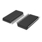 V62/05612-01YE
The activity of extra discounts on wholesale prices is in full swing…
Please fill in your contact information and we will send you the latest wholesale price list.





