 ChipApex | Global Electronic Components Supplier
SEARCH
Search Product
Search Post
— IC芯片 | 连接器 | 传感器 | 被动器件 —
Search productSearch post
— IC芯片 | 连接器 | 传感器 | 被动器件 —
Consult the customer manager about the wholesale price.
consultation hotline:86-132-6715-2157
email:[email protected]
Contact the product manager for consultation. One-stop consultation is available.
Do you want a lower wholesale price? Please send us your inquiry and we will reply immediately.
The V62/13605-01XE is a military-enhanced single 3-input positive OR-AND gate manufactured by Texas Instruments. It operates within a supply voltage range of 1.65 V to 5.5 V and supports defense, aerospace, and medical applications. The device features a maximum propagation delay of 5 ns at 3.3 V and provides ±24 mA output drive capability. It includes input hysteresis for improved noise immunity and Ioff circuitry to support partial-power-down modes. The component is housed in a DBV (SOT-23) package with six pins.
Verify the specific ordering suffix and revision level against the latest Package Option Addendum to ensure compatibility with current manufacturing standards. Confirm that the selected variant meets all required environmental specifications for the intended operational temperature range. Ensure proper handling procedures are followed due to the sensitive nature of the SOT-23 packaging.
Select this component when a compact logic solution is required for high-reliability environments. The device offers flexible logic configurations by tying inputs to ground or supply rails. Consider the low power consumption and wide operating voltage range when designing power-sensitive circuits. Verify thermal requirements based on the junction-to-ambient resistance values provided in the datasheet.
This part belongs to the SN74LVC1G3208-EP family, which is designed for enhanced performance in harsh environments. The 'EP' designation indicates it is an enhanced product suitable for long-term production and traceability. It serves as a specialized alternative to standard catalog versions for critical infrastructure and defense applications requiring extended product life cycles.
The catalog version SN74LVC1G3208 is available but lacks the enhanced reliability features. The automotive qualified version SN74LVC1G3208-Q1 targets zero-defect automotive applications. Direct substitution requires verifying that the replacement meets the specific military environmental and traceability requirements of the original design.
The device incorporates Ioff circuitry that automatically disables the outputs when the device is powered down, preventing damaging current backflow through the component.
By tying specific inputs to GND or VCC, the device can function as a 2-input OR gate or a 2-input AND gate in addition to its primary 3-input OR-AND configuration.
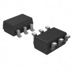 V62/13605-01XE
The activity of extra discounts on wholesale prices is in full swing…
Please fill in your contact information and we will send you the latest wholesale price list.





