 ChipApex | Global Electronic Components Supplier

SEARCH
Search Product
Search Post
— IC芯片 | 连接器 | 传感器 | 被动器件 —
Search productSearch post
— IC芯片 | 连接器 | 传感器 | 被动器件 —
Consult the customer manager about the wholesale price.
consultation hotline:86-132-6715-2157
email:[email protected]
Contact the product manager for consultation. One-stop consultation is available.
Do you want a lower wholesale price? Please send us your inquiry and we will reply immediately.
VF2510BG is listed in the Application Specific Clock/Timing range at ChipApex. The manufacturer field lists Renesas Electronics Corporation. Its product description is IC PLL CLK DRIVER 3.3V 24-TSSOP. Review the specifications below when checking this part for your BOM.
The Renesas VF2510BG is a 3.3V Phase-Lock Loop (PLL) clock driver designed for synchronous SDRAM applications. It distributes one clock input to ten outputs with low skew and jitter, meeting PC133 registered DIMM specifications. The device operates at frequencies from 20MHz to 200MHz within a 2.97V to 3.63V supply range. It features an internal loop filter, eliminating the need for external RC components. The IC is housed in a 24-pin TSSOP package and supports Spread Spectrum Clocking compatibility.
Verify component authenticity through authorized channels as this part may be subject to obsolescence or replacement by newer series variants. Confirm package marking and datasheet revision against current manufacturer documentation prior to procurement to ensure functional compatibility.
Select this component when a single-ended clock source requires expansion to ten loads with precise phase alignment. Ensure the design accommodates the 3.3V supply voltage and utilizes the FBIN/FBOUT terminals for proper PLL synchronization. Verify that the operating temperature range of 0°C to 70°C meets system environmental requirements.
This device belongs to the ICSVF2510 family of clock drivers originally developed by Integrated Circuit Systems, Inc., now part of Renesas Electronics. It serves as a specialized buffer for memory subsystems requiring strict timing constraints and low jitter performance compared to standard fanout buffers.
Check for direct replacements such as the CDCVF2510 series from Texas Instruments which offers similar PLL-based clock buffering functionality in comparable packages.
Explore related parts through Clock/Timing, Integrated Circuits (ICs), all product categories, ChipApex homepage.
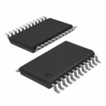 VF2510BG

The activity of extra discounts on wholesale prices is in full swing…
Please fill in your contact information and we will send you the latest wholesale price list.






