 ChipApex | Global Electronic Components Supplier
SEARCH
Search Product
Search Post
— IC芯片 | 连接器 | 传感器 | 被动器件 —
Search productSearch post
— IC芯片 | 连接器 | 传感器 | 被动器件 —
Consult the customer manager about the wholesale price.
consultation hotline:86-132-6715-2157
email:[email protected]
Contact the product manager for consultation. One-stop consultation is available.
Do you want a lower wholesale price? Please send us your inquiry and we will reply immediately.
The VO2630-X009T is a high-speed dual-channel logic output optoisolator manufactured by Vishay Semiconductor Opto Division. It features an LED input and open-drain outputs with Schottky clamping, housed in an 8-SMD package. Key electrical parameters include a data rate of 10 MBd, isolation voltage of 5300 Vrms, and common mode transient immunity of 1 kV/µs. Propagation delays are typically 75 ns max for both low-to-high and high-to-low transitions. The device operates on a supply voltage of 4.5V to 5.5V, supports a maximum forward current of 15 mA, and delivers an output current of 50 mA per channel within a temperature range of -40°C to +100°C.
Verify the specific suffix X009T confirms the 8-SMD surface-mount packaging variant, as standard VO2630 parts may differ in form factor. Confirm RoHS compliance status through official manufacturer documentation prior to integration. Ensure design specifications align with the 5300 Vrms isolation rating and 10 MBd data rate limits defined in the datasheet.
Select this component when dual-channel isolation is required alongside high-speed performance exceeding standard transistor-output optocouplers. The open-drain configuration necessitates external pull-up resistors; verify resistor values match the target logic voltage levels. Consider the 8-SMD footprint constraints during PCB layout to maintain adequate creepage and clearance distances for the specified isolation voltage.
This part belongs to Vishay's high-speed logic output optocoupler family, which utilizes integrated photodetector ICs for superior performance compared to discrete phototransistor designs. The VO2630 series is engineered for applications demanding fast propagation delays and robust noise immunity, distinguishing it from slower general-purpose optocouplers like the 4N26 series.
The VO2630-X009T is functionally equivalent to the 6N137-X009T regarding pinout and electrical characteristics. Verify that any substitute maintains the same 8-SMD package dimensions and open-drain output configuration to ensure direct compatibility without circuit modification.
The maximum propagation delay (tpLH and tpHL) is 75 ns.
Yes, the integrated Schottky-clamped outputs are designed for LVTTTL and LVCMOS compatibility.
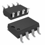 VO2630-X009T
The activity of extra discounts on wholesale prices is in full swing…
Please fill in your contact information and we will send you the latest wholesale price list.





