 ChipApex | Global Electronic Components Supplier
SEARCH
Search Product
Search Post
— IC芯片 | 连接器 | 传感器 | 被动器件 —
Search productSearch post
— IC芯片 | 连接器 | 传感器 | 被动器件 —
Consult the customer manager about the wholesale price.
consultation hotline:86-132-6715-2157
email:[email protected]
Contact the product manager for consultation. One-stop consultation is available.
Do you want a lower wholesale price? Please send us your inquiry and we will reply immediately.
The VSP01M01ZWD is a mixed-signal integrated circuit designed for charge-coupled device (CCD) signal processing in digital cameras. It integrates a CCD timing generator, analog-to-digital converter (ADC), and vertical driver within a BGA-100 package. The device features a 36-MHz correlated double sampling (CDS) channel with programmable gain ranging from -9 dB to +44 dB. The ADC resolution varies by variant: the VSP01M01 provides 10-bit resolution, while the VSP01M02 offers 12-bit resolution, both operating at a 36-MHz conversion rate. Power consumption is specified at 139 mW during normal operation at 3.0 V.
Verify the specific suffix for packaging requirements: ZWD indicates tray packaging, while ZWDR indicates tape and reel. Confirm the base model number, as VSP01M01 provides 10-bit resolution and VSP01M02 provides 12-bit resolution. Check for the 'Not Recommended for New Designs' status on current distributor listings to assess long-term availability constraints.
Select the VSP01M01ZWD for applications requiring 10-bit resolution or the VSP01M02ZWD for 12-bit resolution needs. Ensure the design supports the required supply voltages, specifically the negative VL rail (-5.0 V to -9.0 V) and positive VH rail (11.5 V to 15.5 V). Verify that the serial interface timing parameters align with the host controller's capabilities for register configuration.
This component belongs to Texas Instruments' VSP series of CCD analog front-end processors. It is part of a family that includes variants like the VSP1000 and VSP2267. The datasheet explicitly marks this product as 'Not Recommended for New Designs,' indicating it is a legacy component intended for maintenance of existing designs rather than new development.
Public confirmed substitute part numbers are not available in the provided documentation.
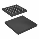 VSP01M01ZWD
The activity of extra discounts on wholesale prices is in full swing…
Please fill in your contact information and we will send you the latest wholesale price list.





