ChipApex | Global Electronic Components Supplier

SEARCH
Search Product
Search Post
— IC芯片 | 连接器 | 传感器 | 被动器件 —
Search productSearch post
— IC芯片 | 连接器 | 传感器 | 被动器件 —
Consult the customer manager about the wholesale price.
consultation hotline:86-132-6715-2157
email:[email protected]
Contact the product manager for consultation. One-stop consultation is available.
Do you want a lower wholesale price? Please send us your inquiry and we will reply immediately.
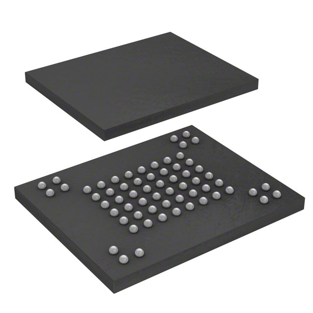
W29N04KZBIBG TR is listed in the Memory IC range at ChipApex. The manufacturer field lists Winbond Electronics. Its product description is IC FLASH 4GBIT ONFI 63VFBGA. Review the specifications below when checking this part for your BOM.
The W29N04KZBIBG TR is a 4G-bit Single-Level Cell NAND flash memory manufactured by Winbond Electronics. It operates on a single 1.7V to 1.95V power supply and features an x8 data bus width. The device is housed in a 63-ball VFBGA package with a 9x11mm footprint. It supports standard NAND interfaces and includes hardware write protection via the #WP pin. The memory array consists of 2,048 blocks, each containing 64 pages of 4,352 bytes. It offers high endurance of 60,000 erase/program cycles and a 10-year data retention capability.
Verify the specific suffix 'TR' indicates reel packaging when sourcing. Confirm the 'B' package code corresponds to the 63-ball VFBGA form factor required for your PCB layout. Ensure the voltage range matches your system's 1.8V rail specifications. Check for moisture sensitivity level requirements during assembly processing.
Select this component for designs requiring high density in a compact surface-mount package. The x8 interface suits systems with narrower data buses. Consider the industrial temperature range if operating in extreme environments. Verify that the host controller supports the specific command set and timing parameters defined in the datasheet.
This part belongs to the W29N04KW/ZxxBG family from Winbond. It is designed as a cost-effective solution for embedded storage needs. The family shares core electrical characteristics but varies in package type and temperature rating. The W29N04KZBIBG specifically denotes the industrial grade version in the VFBGA package.
Direct replacements must match the 4G-bit density, 1.8V operation, and 63-ball VFBGA package. Verify compatibility with existing firmware drivers due to potential differences in parameter page structures or timing constraints between manufacturers.
The #WP pin provides hardware write protection. When active low, it disables all program and erase operations to prevent accidental data modification.
The memory is organized into 2,048 erasable blocks. Each block contains 64 programmable pages, with each page sized at 4,352 bytes (4,096 bytes main data plus 256 bytes spare area).
Explore related parts through Memory, Integrated Circuits (ICs), all product categories, ChipApex homepage.
 W29N04KZBIBG TR

The activity of extra discounts on wholesale prices is in full swing…
Please fill in your contact information and we will send you the latest wholesale price list.