 ChipApex | Global Electronic Components Supplier

SEARCH
Search Product
Search Post
— IC芯片 | 连接器 | 传感器 | 被动器件 —
Search productSearch post
— IC芯片 | 连接器 | 传感器 | 被动器件 —
Consult the customer manager about the wholesale price.
consultation hotline:86-132-6715-2157
email:[email protected]
Contact the product manager for consultation. One-stop consultation is available.
Do you want a lower wholesale price? Please send us your inquiry and we will reply immediately.
W40S11-02H is listed in the Application Specific Clock/Timing range at ChipApex. The manufacturer field lists Infineon Technologies. Its product description is IC CLK BUFF 10OUT SDRAM 28SSOP. Review the specifications below when checking this part for your BOM.
The W40S11-02 is a low-voltage, ten-output clock buffer designed for driving SDRAM DIMMs in mobile systems. It features skew-controlled CMOS outputs with an impedance of approximately 15 Ω and propagation delays between 1.0 to 5.0 ns. The device operates on a single 3.3V supply and supports frequencies up to 133 MHz. It includes an I²C serial configuration interface for output control and utilizes a 28-pin SSOP package.
Verify the manufacturer origin, as the datasheet identifies Cypress Semiconductor Corporation while the model query specifies Infineon Technologies. Confirm the package type matches the required 28-pin SSOP or TSSOP variant. Ensure the operating temperature range of 0°C to +70°C meets system requirements.
Select this component when a ten-channel clock buffer with precise skew control (<250 ps) is required for SDRAM applications. The 15 Ω output impedance is optimized for DIMM loads. Consider the I²C interface if dynamic output control is needed. Verify compatibility with the 3.3V logic levels and 133 MHz maximum frequency.
This component was originally manufactured by Cypress Semiconductor Corporation. The datasheet indicates it is ideal for high-performance systems designed around Intel’s latest Mobile chipset at the time of publication. It serves as a specialized buffer for memory clock signals rather than a general-purpose logic gate.
Check for direct cross-references from Infineon Technologies if the brand specification is mandatory. Verify pinout and electrical parameters against other ten-channel SDRAM buffers if substituting with generic equivalents.
Outputs can be controlled via the OE pin (three-stated when LOW) or through the I²C serial interface, which allows individual enable/disable configuration for each of the ten outputs.
The nominal output buffer impedance is 15 ohms, which is designed to be ideal for driving SDRAM DIMMs.
The specific slave receiver address for the W40S11-02 is 11010010.
Explore related parts through Clock/Timing, Integrated Circuits (ICs), all product categories, ChipApex homepage.
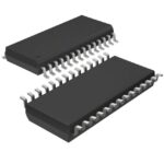 W40S11-02H

The activity of extra discounts on wholesale prices is in full swing…
Please fill in your contact information and we will send you the latest wholesale price list.





