 ChipApex | Global Electronic Components Supplier
SEARCH
Search Product
Search Post
— IC芯片 | 连接器 | 传感器 | 被动器件 —
Search productSearch post
— IC芯片 | 连接器 | 传感器 | 被动器件 —
Consult the customer manager about the wholesale price.
consultation hotline:86-132-6715-2157
email:[email protected]
Contact the product manager for consultation. One-stop consultation is available.
Do you want a lower wholesale price? Please send us your inquiry and we will reply immediately.
The W681310WG is a single-channel PCM CODEC designed for voiceband applications, operating from a single +3V power supply (2.7V to 5.25V). It features pin-selectable μ-Law or A-Law companding compliant with ITU G.711 and filtering compliant with ITU G.712. The device includes an on-chip precision voltage reference and push-pull power amplifiers capable of driving 300Ω loads differentially up to 3.544V peak-to-peak. It supports eight master clock rates between 256 kHz and 4.800 MHz via an internal pre-scaler. Performance is specified over the industrial temperature range of –40°C to +85°C in a 20-pin TSSOP package.
Verify the specific suffix 'WG' corresponds to the 20-pin TSSOP package variant when sourcing. Confirm RoHS compliance status through official manufacturer documentation prior to integration. Ensure that the ordering information matches the exact revision level required for your application to avoid potential discrepancies in electrical characteristics or pinout definitions.
Select this component for designs requiring a single-supply voiceband codec with integrated output drivers. Verify that the system master clock falls within the supported range of 256 kHz to 4.800 MHz. Ensure the load impedance requirements align with the differential amplifier capabilities. Consider the industrial temperature range if the deployment environment involves extreme thermal conditions.
The W681310 series comprises general-purpose single-channel PCM CODECs available in various packages including SOG, SSOP, and TSSOP. The WG suffix specifically denotes the 20-pin Thin Shrink Small Outline Package (TSSOP) variant. This family is designed for cost-effective voice processing solutions in telecommunications and consumer electronics.
Direct pin-compatible replacements are not explicitly listed in the provided datasheet. Evaluate alternative Nuvoton voiceband codecs based on package compatibility and interface protocol support. Verify that any substitute component meets the same ITU-T G.711 and G.712 compliance standards.
The companding format is selected via the μ/A-Law pin. Connecting this pin to VDD selects μ-Law, while connecting it to VSS selects A-Law.
The PUI pin is the Power Up input signal. Tying it to VDD powers up the part, while tying it to VSS puts the part into power-down mode.
Yes, the transmit power amplifier can be powered down by connecting the PAI pin to VDD when it is not in use.
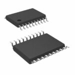 W681310WG
The activity of extra discounts on wholesale prices is in full swing…
Please fill in your contact information and we will send you the latest wholesale price list.







