 ChipApex | Global Electronic Components Supplier
SEARCH
Search Product
Search Post
— IC芯片 | 连接器 | 传感器 | 被动器件 —
Search productSearch post
— IC芯片 | 连接器 | 传感器 | 被动器件 —
Consult the customer manager about the wholesale price.
consultation hotline:86-132-6715-2157
email:[email protected]
Contact the product manager for consultation. One-stop consultation is available.
Do you want a lower wholesale price? Please send us your inquiry and we will reply immediately.
The W682310 is a dual-channel voiceband PCM CODEC compliant with ITU G.712 and G.711 specifications. It operates from a single +3V power supply (2.7V to 3.8V) and features pin-selectable μ-Law or A-Law companding. The device integrates two complete analog-to-digital and digital-to-analog paths, each including anti-aliasing and smoothing filters. An internal PLL eliminates the need for an external master clock by automatically determining the division ratio for required internal clocks based on the frame sync frequency. Typical power dissipation is 35 mW, reducing to 5 μW in power-down mode.
Verify component authenticity through authorized distributors or direct manufacturer channels. Confirm package availability as options include SSOP and SOP variants. Ensure design compatibility with the specific 2.7V to 3.8V operating voltage range. Review latest datasheet revisions for any updates to electrical characteristics or pin configurations before finalizing procurement orders.
Select the W682310 when a low-voltage single-supply operation is required compared to the W682510 variant. Verify that the system supports the 2.7V to 3.8V input range. Consider the integrated PLL functionality if external clock generation components are to be minimized. Ensure the application requires dual-channel processing capabilities within the specified industrial temperature range.
The W682310 belongs to the W682xx series of general-purpose dual-channel PCM CODECs manufactured by Nuvoton Technology Corporation. This series includes the W682510, which shares identical functional architecture but operates at a higher +5V supply voltage. Both devices target voiceband applications requiring standardized companding and filtering.
The W682510 serves as a functional alternative if the system design utilizes a +5V supply instead of +3V. Pinout compatibility exists between the variants, though supply voltage constraints must be strictly observed. No other direct substitutes are documented in the official datasheet.
The companding format is selected via the μ/A-Law pin. Connecting this pin to VDD selects A-Law, while connecting it to VSSA or leaving it floating selects μ-Law.
The Power Up Input (PUI) pin controls the power state. Setting PUI to logic HIGH powers up the device, while setting it to logic LOW places all internal circuits into power-down mode.
No, the device contains a built-in Phase Locked Loop (PLL) that eliminates the need for a master clock. It automatically determines the division ratio for the required internal clock based on the frame sync frequency.
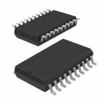 W682310R
The activity of extra discounts on wholesale prices is in full swing…
Please fill in your contact information and we will send you the latest wholesale price list.







