 ChipApex | Global Electronic Components Supplier
SEARCH
Search Product
Search Post
— IC芯片 | 连接器 | 传感器 | 被动器件 —
Search productSearch post
— IC芯片 | 连接器 | 传感器 | 被动器件 —
Consult the customer manager about the wholesale price.
consultation hotline:86-132-6715-2157
email:[email protected]
Contact the product manager for consultation. One-stop consultation is available.
Do you want a lower wholesale price? Please send us your inquiry and we will reply immediately.
The WM1824BGEDT/R is a stereo digital-to-analog converter (DAC) featuring an integrated charge pump for generating 2Vrms ground-referenced line outputs from a single 3.3V supply. It supports audio sampling rates from 8kHz to 192kHz via an I2S slave interface and utilizes hardware control for mute functions. Key electrical specifications include a signal-to-noise ratio of 106dB (A-weighted), total harmonic distortion of -87dB at -1dBFS, and channel separation of 100dB at 1kHz. The device operates within a temperature range of -40°C to +85°C and is housed in a 16-lead TSSOP package.
Verify the ordering code WM1824BGEDT/R against the manufacturer's production data to confirm the tape and reel packaging configuration. Ensure that the moisture sensitivity level (MSL1) requirements are met for storage and handling prior to surface mount assembly. Confirm that the lead-free status aligns with specific project environmental regulations.
Select this component when a ground-referenced output is required without external coupling capacitors. The integrated DC servo eliminates power-on pops and clicks, simplifying the design for consumer audio applications. Ensure the system logic levels are compatible with the 3.3V tolerant digital interface and that the available master clock frequencies support the desired sampling rates.
The WM1824B series was originally developed by Wolfson Microelectronics plc before being acquired by Cirrus Logic. The datasheet revision history indicates updates to order codes and performance parameters between 2010 and 2012. This part represents a high-fidelity stereo DAC solution designed for cost-sensitive consumer electronics requiring minimal external components.
Publicly confirmed substitute part numbers are not provided in the source documentation. Designers should consult official cross-reference lists or application notes for equivalent devices with similar pinouts and performance characteristics.
The WM1824B uses an internal DC servo to eliminate the need for line driving coupling capacitors and effectively eliminates power-on pops and clicks through its suppressed power-up/down sequencer.
To prevent over-current protection shutdown, the load impedance must never be less than 100Ω. The standard test condition specifies a load impedance of 1kΩ.
Yes, the DBVDD can operate at either 1.8V or 3.3V, while AVDD and LINEVDD operate at 3.3V ±10%. The digital interface is 3.3V tolerant.
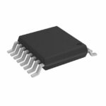 WM1824BGEDT/R
The activity of extra discounts on wholesale prices is in full swing…
Please fill in your contact information and we will send you the latest wholesale price list.






