 ChipApex | Global Electronic Components Supplier
SEARCH
Search Product
Search Post
— IC芯片 | 连接器 | 传感器 | 被动器件 —
Search productSearch post
— IC芯片 | 连接器 | 传感器 | 被动器件 —
Consult the customer manager about the wholesale price.
consultation hotline:86-132-6715-2157
email:[email protected]
Contact the product manager for consultation. One-stop consultation is available.
Do you want a lower wholesale price? Please send us your inquiry and we will reply immediately.
The XC18V01PCG20C0100 is a member of the Xilinx XC18V00 series, specifically the 1-megabit (XC18V01) in-system programmable configuration PROM. It utilizes a low-power advanced CMOS FLASH process and operates at 3.3V with 5V-tolerant I/O pins. The device supports dual configuration modes: serial (up to 33 MHz) and parallel (up to 264 Mb/s). It features IEEE Std 1149.1 JTAG support for boundary-scan testing and in-system programming, offering an endurance of 20,000 program/erase cycles and data retention of 20 years.
This component is officially marked as Obsolete or Under Obsolescence by the manufacturer. Verify current availability status through authorized distributors. Ensure compatibility with legacy Xilinx development tools such as ISE Foundation. Confirm that the specific PCG20 package variant meets the mechanical requirements of the target PCB design before procurement.
Select this device when configuring Xilinx FPGAs requiring approximately 1 megabit of non-volatile storage. The PCG20 suffix indicates a 20-pin Plastic Leaded Chip Carrier package. Ensure the target FPGA supports Master Serial mode or requires external clocking for Slave modes. Verify voltage levels match the 3.3V VCCINT and VCCO specifications.
The XC18V00 series serves as a dedicated configuration memory solution for various Xilinx FPGA and CPLD families. These devices replace older OTP PROMs by offering reprogrammability and higher density. The XC18V01 specifically targets designs needing 1 Megabit capacity, bridging the gap between smaller 512-kilobit and larger 2-megabit options within the same pin-compatible family.
Official substitutes include other members of the XC18V00 series such as XC18V02, XC18V04, or XC18V512, depending on required bitstream size. Cross-family replacements may require schematic changes due to pinout differences. Consult Xilinx documentation for compatible FPGA lists to ensure functional equivalence.
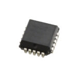 XC18V01PCG20C0100
The activity of extra discounts on wholesale prices is in full swing…
Please fill in your contact information and we will send you the latest wholesale price list.





