 ChipApex | Global Electronic Components Supplier
SEARCH
Search Product
Search Post
— IC芯片 | 连接器 | 传感器 | 被动器件 —
Search productSearch post
— IC芯片 | 连接器 | 传感器 | 被动器件 —
Consult the customer manager about the wholesale price.
consultation hotline:86-132-6715-2157
email:[email protected]
Contact the product manager for consultation. One-stop consultation is available.
Do you want a lower wholesale price? Please send us your inquiry and we will reply immediately.
The XC18V512PC20I is a 3.3V in-system programmable configuration PROM from the Xilinx XC18V00 series, housed in a 20-pin PLCC package. It provides 512-kilobit storage capacity for Xilinx FPGA bitstreams. The device supports serial and parallel configuration modes, featuring IEEE 1149.1 JTAG boundary-scan compliance for programming and testing. It offers 20,000 program/erase cycle endurance and operates across commercial and industrial temperature ranges.
Verify the package type matches the required PCB footprint, as the PC20 suffix denotes a 20-pin PLCC. Confirm voltage requirements align with the 3.3V VCCINT and VCCO specifications. Ensure design tools support the specific IDCODE associated with this density level for proper identification during in-system programming.
Select this component when a non-volatile memory solution is needed for FPGA configuration without external microcontrollers. It is suitable for designs requiring reprogrammability in the field. Consider cascading multiple units if the target FPGA configuration size exceeds 512 kilobits. Verify compatibility with the specific FPGA family's master or slave mode requirements.
This part belongs to the XC18V00 series of in-system programmable PROMs designed specifically for Xilinx FPGA configuration. The series includes various densities ranging from 512-kilobit to 4-megabit. These devices replace older OTP PROMs by allowing repeated reprogramming, facilitating design iterations and field updates without replacing the physical chip.
XC18V512PQ20C
The 20-pin packages do not have a dedicated CF pin. The CF function can be routed to pin 7 by setting the CF --> D4 option, provided the parallel output mode is not used.
The Chip Enable Output (CEO) drives the CE input of the next PROM in a daisy chain, allowing multiple devices to be concatenated for storing larger configuration bitstreams.
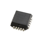 XC18V512PC20I
The activity of extra discounts on wholesale prices is in full swing…
Please fill in your contact information and we will send you the latest wholesale price list.





