ChipApex | Global Electronic Components Supplier

SEARCH
Search Product
Search Post
— IC芯片 | 连接器 | 传感器 | 被动器件 —
Search productSearch post
— IC芯片 | 连接器 | 传感器 | 被动器件 —
Consult the customer manager about the wholesale price.
consultation hotline:86-132-6715-2157
email:[email protected]
Contact the product manager for consultation. One-stop consultation is available.
Do you want a lower wholesale price? Please send us your inquiry and we will reply immediately.
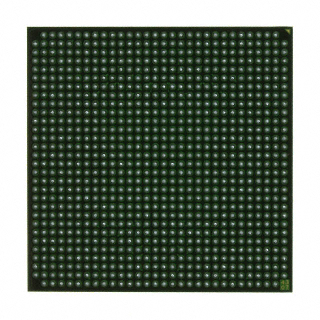
XC2V1000-4FFG896I is listed in the Field Programmable Gate Array range at ChipApex. The manufacturer field lists AMD. Its product description is IC FPGA 432 I/O 896FCBGA. Review the specifications below when checking this part for your BOM.
The AMD XC2V1000-4FFG896I is a Virtex-II series Field Programmable Gate Array (FPGA) manufactured using a 0.15 µm CMOS process with 8-layer metal interconnects. It features 1,000,000 system gates and an array of 40 x 32 Configurable Logic Blocks (CLBs), totaling 5,120 slices. The device provides up to 432 user I/O pads via the FF896 flip-chip fine-pitch BGA package. Internal resources include forty 18-Kb Block SelectRAM blocks for dual-port memory and dedicated 18-bit x 18-bit multiplier blocks. It supports high-speed interfaces including LVDS and DDR standards.
Verify the specific ordering suffix against official documentation to confirm temperature range and package type. The 'I' suffix indicates industrial temperature rating (-40°C to +100°C). Confirm that the FF896 designation corresponds to the required flip-chip fine-pitch BGA package. Ensure compatibility with existing design footprints before procurement.
Select this component when designs require approximately one million system gates with high-density I/O capabilities. The FF896 package is suitable for applications needing up to 432 user I/Os in a compact form factor. Consider the availability of 18-Kb Block RAM and multipliers for embedded memory and arithmetic functions. Verify that the speed grade meets the timing requirements of the target application.
This device belongs to the Virtex-II family, which was designed as a platform FPGA solution based on IP cores and customized modules. The family ranges from 40K to 8M system gates, utilizing a leading-edge 0.15 µm / 0.12 µm CMOS process optimized for high speed and low power consumption. It serves as a powerful alternative to mask-programmed gate arrays for complex logic designs.
Public confirmed substitute part numbers are not available in the provided source material.
Explore related parts through Embedded, Integrated Circuits (ICs), all product categories, ChipApex homepage.
 XC2V1000-4FFG896I

The activity of extra discounts on wholesale prices is in full swing…
Please fill in your contact information and we will send you the latest wholesale price list.