 ChipApex | Global Electronic Components Supplier

SEARCH
Search Product
Search Post
— IC芯片 | 连接器 | 传感器 | 被动器件 —
Search productSearch post
— IC芯片 | 连接器 | 传感器 | 被动器件 —
Consult the customer manager about the wholesale price.
consultation hotline:86-132-6715-2157
email:[email protected]
Contact the product manager for consultation. One-stop consultation is available.
Do you want a lower wholesale price? Please send us your inquiry and we will reply immediately.
XC2V1500-5FGG676I is listed in the Field Programmable Gate Array range at ChipApex. The manufacturer field lists AMD. Its product description is IC FPGA 392 I/O 676FBGA. Review the specifications below when checking this part for your BOM.
The XC2V1500-5FGG676I is a Virtex-II Platform FPGA manufactured by Xilinx, utilizing a 0.15 µm CMOS process with 8-layer metal interconnects. It features 1.5 million system gates and 7,680 configurable logic blocks (CLBs). The device provides up to 528 user I/O pads in the FG676 flip-chip package. Internal resources include 48 multiplier blocks, 864 Kbits of block SelectRAM, and 8 Digital Clock Manager (DCM) modules. The core operates at 1.5 V, while auxiliary supplies support 3.3 V I/O standards.
Verify component authenticity through authorized distributors or original manufacturer channels. Confirm that the specific ordering suffix matches the required temperature grade and package type. Ensure compliance with RoHS directives if lead-free packaging is mandated for the assembly process.
Select this model when designs require approximately 1.5 million system gates within a fine-pitch BGA footprint. Compare against lower-density members like the XC2V1000 for cost optimization or higher-density options like the XC2V2000 for expanded logic capacity. Verify that the 528 I/O limit satisfies interface requirements.
This component belongs to the Virtex-II family, representing a platform FPGA solution optimized for high-speed applications. It bridges the gap between mid-range density devices and larger multi-million gate arrays, offering a balance of performance and resource availability for complex logic implementations.
Direct pin-compatible replacements within the same package are limited due to the specific speed grade and density. Consider the XC2V1500-5FF896I for a flip-chip alternative with increased I/O count, or the XC2V1000-5FGG676I for a lower-cost option with reduced logic resources.
In the FG676 wire-bond package, the XC2V1500 supports up to 392 user I/Os. In the FF896 flip-chip package, it supports up to 528 user I/Os.
The XC2V1500 contains 8 DCM modules for clock distribution and management.
The internal core supply voltage (VCCINT) is 1.5 V.
Explore related parts through Embedded, Integrated Circuits (ICs), all product categories, ChipApex homepage.

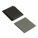 XC2V1500-5FGG676I

The activity of extra discounts on wholesale prices is in full swing…
Please fill in your contact information and we will send you the latest wholesale price list.





