 ChipApex | Global Electronic Components Supplier
SEARCH
Search Product
Search Post
— IC芯片 | 连接器 | 传感器 | 被动器件 —
Search productSearch post
— IC芯片 | 连接器 | 传感器 | 被动器件 —
Consult the customer manager about the wholesale price.
consultation hotline:86-132-6715-2157
email:[email protected]
Contact the product manager for consultation. One-stop consultation is available.
Do you want a lower wholesale price? Please send us your inquiry and we will reply immediately.
The XC7SET125GM,115 is a high-speed silicon-gate CMOS bus buffer and line driver featuring one non-inverting channel with three-state output capability. It operates within a supply voltage range of 4.5 V to 5.5 V. The device provides symmetrical output impedance and balanced propagation delays. It supports TTL input levels and includes electrostatic discharge protection exceeding 2000 V (HBM) and 1000 V (CDM). The component is specified for operation from -40 °C to +125 °C and utilizes the XSON6 package.
Verify the specific ordering suffix
Select this component when a single-channel, non-inverting buffer with three-state output is required. Ensure the application operates within the 4.5 V to 5.5 V supply voltage range. Consider the XSON6 package dimensions if space constraints are critical. Verify that the required operating temperature range extends to +125 °C, as this variant supports that upper limit.
The XC7SET125 series consists of high-speed Si-gate CMOS devices designed for bus buffering and line driving. The family includes variants with different package options such as TSSOP5, SC-74A, and XSON6. All variants share the same functional characteristics, providing a single non-inverting buffer with three-state output. The series is optimized for low power dissipation and high noise immunity.
XC7SET125GW,115; XC7SET125GV,115
The three-state output is controlled by the output enable input (OE). A HIGH level at OE causes the output to assume a high-impedance OFF-state.
The recommended operating condition specifies a maximum supply voltage of 5.5 V, while the absolute maximum rating allows up to 7.0 V.
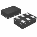 XC7SET125GM,115
The activity of extra discounts on wholesale prices is in full swing…
Please fill in your contact information and we will send you the latest wholesale price list.





