 ChipApex | Global Electronic Components Supplier
SEARCH
Search Product
Search Post
— IC芯片 | 连接器 | 传感器 | 被动器件 —
Search productSearch post
— IC芯片 | 连接器 | 传感器 | 被动器件 —
Consult the customer manager about the wholesale price.
consultation hotline:86-132-6715-2157
email:[email protected]
Contact the product manager for consultation. One-stop consultation is available.
Do you want a lower wholesale price? Please send us your inquiry and we will reply immediately.
The XC7SET125GW,125 is a high-speed Si-gate CMOS bus buffer and line driver featuring one non-inverting channel with 3-state output. It operates within a supply voltage range of 4.5 V to 5.5 V and supports an ambient temperature range from -40 °C to +125 °C. The device provides symmetrical output impedance, balanced propagation delays, and TTL input levels. Static characteristics include a maximum supply current of 40 μA at 5.5 V and low input leakage. Dynamic performance specifies a typical propagation delay of 4.8 ns at 50 pF load.
Verify the specific ordering suffix
Select this component when a single-channel, non-inverting buffer with 3-state capability is required for 5V logic systems. Ensure the design accommodates the TSSOP5 package dimensions and thermal derating requirements above 74 °C. Confirm that the application voltage remains within the 4.5 V to 5.5 V recommended operating range to maintain specified timing and static parameters.
This part belongs to the Nexperia XC7SET125 family of bus buffers and line drivers. The family includes variants with different packages such as SC-74A (GV) and XSON6 (GM), all sharing identical electrical specifications. The XC7SET125 series is designed for high-speed CMOS applications, offering balanced propagation delays and robust ESD protection suitable for demanding industrial and commercial environments.
XC7SET125GV,125 (SC-74A package)
The output enters a high-impedance OFF-state when the Output Enable (OE) input is HIGH. When OE is LOW, the output follows the data input A.
The absolute maximum supply voltage (VCC) is 7.0 V, but the recommended operating range is 4.5 V to 5.5 V.
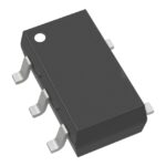 XC7SET125GW,125
The activity of extra discounts on wholesale prices is in full swing…
Please fill in your contact information and we will send you the latest wholesale price list.





