 ChipApex | Global Electronic Components Supplier

SEARCH
Search Product
Search Post
— IC芯片 | 连接器 | 传感器 | 被动器件 —
Search productSearch post
— IC芯片 | 连接器 | 传感器 | 被动器件 —
Consult the customer manager about the wholesale price.
consultation hotline:86-132-6715-2157
email:[email protected]
Contact the product manager for consultation. One-stop consultation is available.
Do you want a lower wholesale price? Please send us your inquiry and we will reply immediately.
The XC7SH32GW,125 is a high-speed Si-gate CMOS device providing a single 2-input OR logic function. It operates within a supply voltage range of 2.0 V to 5.5 V and supports an input voltage up to 5.5 V. The component features symmetrical output impedance and balanced propagation delays, with typical values of 4.6 ns at 5.0 V and 5.5 ns at 3.3 V under a 50 pF load. It includes ESD protection exceeding 2000 V (HBM) and 1000 V (CDM). Designed for surface-mount applications, it utilizes the TSSOP-5 package (SOT353-1) and functions reliably across an ambient temperature range of -40 °C to +125 °C.
Verify the specific ordering suffix
Select this component when a single 2-input OR gate is required in a compact SMD footprint. Ensure the design accommodates the 2.0 V to 5.5 V supply range and the -40 °C to +125 °C operating temperature. Consider the TSSOP-5 package dimensions for PCB layout constraints and verify that the 8 mA output drive capability meets the load requirements.
The XC7SH32 belongs to the Nexperia XC7 series, which encompasses high-speed CMOS logic gates. This series is characterized by advanced BiCMOS or CMOS technologies designed for low power consumption and high noise immunity. The XC7SH32 specifically addresses the need for basic combinational logic in space-constrained designs, offering performance comparable to standard TTL levels while operating at lower voltages.
The XC7SH32GV,125 serves as a functional substitute, offering identical electrical characteristics but housed in an SC-74A (SOT753) package instead of the TSSOP-5. Designers must account for pin-to-pin compatibility differences and physical footprint variations when transitioning between these package types.
The maximum input voltage (VI) is rated at 5.5 V, which allows interfacing with 5 V logic systems even when the device is powered at lower voltages.
No, the XC7SH32 does not include I_OFF circuitry. Therefore, it is not specified for partial power-down applications where backflow current prevention is required.
Propagation delay (tpd) represents both the low-to-high (tPLH) and high-to-low (tPHL) transitions. Typical values are 4.6 ns at VCC = 5.0 V and 5.5 ns at VCC = 3.3 V, measured with a 50 pF load capacitance.
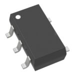 XC7SH32GW,125

The activity of extra discounts on wholesale prices is in full swing…
Please fill in your contact information and we will send you the latest wholesale price list.





