 ChipApex | Global Electronic Components Supplier

SEARCH
Search Product
Search Post
— IC芯片 | 连接器 | 传感器 | 被动器件 —
Search productSearch post
— IC芯片 | 连接器 | 传感器 | 被动器件 —
Consult the customer manager about the wholesale price.
consultation hotline:86-132-6715-2157
email:[email protected]
Contact the product manager for consultation. One-stop consultation is available.
Do you want a lower wholesale price? Please send us your inquiry and we will reply immediately.
XCV300-6FG456C is listed in the Field Programmable Gate Array range at ChipApex. The manufacturer field lists AMD. Its product description is IC FPGA 312 I/O 456FBGA. Review the specifications below when checking this part for your BOM.
The XCV300-6FG456C is a Virtex Field Programmable Gate Array featuring 322,970 system gates and a 32x48 CLB array. It supports up to 312 user I/Os in the FG456 package with a maximum clock frequency of 200 MHz. The device operates at 2.5 V with a commercial temperature range of 0°C to +85°C.
This component is officially listed as obsolete or under obsolescence. Verify current availability status through authorized distributors. Confirm that legacy design files remain compatible with modern development tools if migration is required.
Select this model for designs requiring high-density logic within the original Virtex family. Ensure the FG456 package fits the PCB footprint. Verify that the 2.5 V core voltage and specific I/O banking requirements match the target system power rails.
Part of the original Virtex family utilizing a 0.22 μm five-layer metal CMOS process. This series established high-performance benchmarks for early FPGA implementations before subsequent generations introduced lower voltages and higher densities.
XCV300E-6FG456I
The device supports synchronous system clock rates up to 200 MHz.
The XCV300 provides 65,536 bits of total Block SelectRAM organized into 16 blocks.
Yes, all Virtex IOBs support IEEE 1149.1-compatible boundary scan testing.
Explore related parts through Embedded, Integrated Circuits (ICs), all product categories, ChipApex homepage.
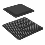 XCV300-6FG456C

The activity of extra discounts on wholesale prices is in full swing…
Please fill in your contact information and we will send you the latest wholesale price list.





