 ChipApex | Global Electronic Components Supplier
SEARCH
Search Product
Search Post
— IC芯片 | 连接器 | 传感器 | 被动器件 —
Search productSearch post
— IC芯片 | 连接器 | 传感器 | 被动器件 —
Consult the customer manager about the wholesale price.
consultation hotline:86-132-6715-2157
email:[email protected]
Contact the product manager for consultation. One-stop consultation is available.
Do you want a lower wholesale price? Please send us your inquiry and we will reply immediately.
The XCZU5EV-L2SFVC784E is a Zynq UltraScale+ MPSoC device from the EV series, manufactured by AMD. It integrates a quad-core ARM Cortex-A53 processor subsystem with dual-core ARM Cortex-R5 processors and an ARM Mali-400 MP2 GPU on a single die. The FPGA fabric provides over 256K logic cells for programmable logic applications. Key specifications include up to 252 user I/Os, 16 GTY transceivers, and 4.5 Mbits of embedded block RAM. The device operates within a junction temperature range of -40°C to 100°C and utilizes a 784-ball FCBGA package.
This component belongs to the Zynq UltraScale+ MPSoC EV family, which targets cost-sensitive industrial and commercial markets. The 'L2' speed grade indicates specific timing characteristics relative to other variants in the XCZU5EV series, while the 'E' suffix denotes the extended commercial temperature range. It shares the same physical package and core architecture as higher-speed or automotive-grade counterparts but differs in performance bins and qualification standards.
Direct pin-to-pin replacements within the same package may include other XCZU5EV variants such as XCZU5EV-1SFVC784E or XCZU5EV-2SFVC784I, provided the speed grade and temperature rating meet system requirements. Cross-series substitutions are not guaranteed due to architectural differences.
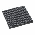 XCZU5EV-L2SFVC784E
The activity of extra discounts on wholesale prices is in full swing…
Please fill in your contact information and we will send you the latest wholesale price list.




