 ChipApex | Global Electronic Components Supplier
SEARCH
Search Product
Search Post
— IC芯片 | 连接器 | 传感器 | 被动器件 —
Search productSearch post
— IC芯片 | 连接器 | 传感器 | 被动器件 —
Consult the customer manager about the wholesale price.
consultation hotline:86-132-6715-2157
email:[email protected]
Contact the product manager for consultation. One-stop consultation is available.
Do you want a lower wholesale price? Please send us your inquiry and we will reply immediately.
The XCZU7EG-L1FBVB900I is an industrial-grade System-on-Chip FPGA from the AMD Xilinx Zynq UltraScale+ MPSoC Enhanced Graphics (EG) family. It integrates a Processing System with quad-core ARM Cortex-A53 processors, dual-core ARM Cortex-R5 processors, and an ARM Mali-400 MP2 GPU, alongside programmable logic resources. The device features approximately 504,000 logic cells, 28,800 Adaptive Logic Modules, and 11 Mbit of embedded memory. It operates within a temperature range of -40°C to +100°C and utilizes a 900-ball FCBGA package.
Verify the specific suffix 'L1' against official AMD documentation to confirm it denotes a standard or low-power variant, as suffix definitions can vary by generation. Ensure compatibility with required I/O standards and power delivery specifications for the target PCB design. Confirm moisture sensitivity level handling requirements during assembly.
Select this model when both high-level application processing via Cortex-A53 and deterministic real-time control via Cortex-R5 are required on a single chip. The EG series is suitable for applications needing enhanced graphics capabilities compared to the EV series. Evaluate the 504K logic cell count against algorithm complexity to ensure sufficient programmable resources for custom hardware acceleration.
This component belongs to the Zynq UltraScale+ MPSoC EG series, which targets high-performance embedded vision and industrial applications. It differs from the EV series by offering enhanced graphics processing capabilities through the Mali-400 MP2 GPU. The 'I' suffix indicates industrial temperature rating, while 'L1' typically specifies a particular binning or power configuration within the EG family.
Direct pin-to-pin replacements within the same package may include other XCZU7EG variants such as XCZU7EG-1FBVB900I or XCZU7EG-2FBVB900I, depending on speed grade and feature set requirements. Cross-series migration to EV models requires verification of GPU availability and logic resource equivalence.
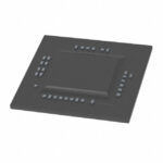 XCZU7EG-L1FBVB900I
The activity of extra discounts on wholesale prices is in full swing…
Please fill in your contact information and we will send you the latest wholesale price list.




