ChipApex | Global Electronic Components Supplier
SEARCH
Search Product
Search Post
— IC芯片 | 连接器 | 传感器 | 被动器件 —
Search productSearch post
— IC芯片 | 连接器 | 传感器 | 被动器件 —
Consult the customer manager about the wholesale price.
consultation hotline:86-132-6715-2157
email:[email protected]
Contact the product manager for consultation. One-stop consultation is available.
Do you want a lower wholesale price? Please send us your inquiry and we will reply immediately.
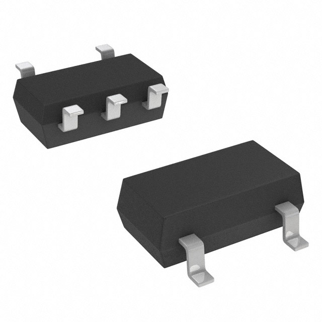
The XN01112 is a composite transistor device manufactured by Panasonic Electronic Components, designed for switching and digital circuits. It integrates two PNP epitaxial planar transistors with built-in bias resistors into a single SC-74A (Mini5-G1) package. The component features a collector-emitter voltage rating of -50 V and a maximum collector current of -100 mA per element. Total power dissipation is rated at 300 mW. Key electrical characteristics include a forward current transfer ratio (hFE) of 60 at -5 mA and an input resistance of 22 kΩ. The transition frequency is specified at 80 MHz.
Verify the specific lifecycle status of the XN01112 directly with Panasonic or authorized distributors before procurement. The datasheet indicates maintenance or discontinuation plans may apply. Confirm that the SC-74A package availability aligns with long-term supply requirements. Ensure compliance with RoHS directives if required for the target application environment.
Select this component when space-saving integration of dual PNP transistors with fixed bias ratios is required. The internal resistor ratio allows for simplified circuit design compared to discrete components. Verify that the -50 V voltage rating and -100 mA current limits meet the specific load requirements of the switching application.
This part belongs to the XN series of composite transistors from Panasonic. These devices are engineered to replace multiple discrete components, offering a compact solution for digital logic applications. The XN01112 specifically utilizes PNP technology, contrasting with NPN variants in the same family.
The datasheet identifies UNR2112 (UN2112) as the conventional equivalent part number. Designers should verify pinout compatibility and electrical parameter tolerances when substituting with other dual PNP composite transistors from different manufacturers.
The device contains two PNP transistors (Tr1 and Tr2) coupled with built-in resistors. Pin 1 and 2 are collectors, Pin 3 is the base of Tr2, Pin 4 is the emitter, and Pin 5 is the base of Tr1.
The nominal input resistance (R1) is 22 kΩ, with a tolerance range of -30% to +30%.
The maximum collector-base cutoff current (ICBO) is 0.1 µA when VCB is -50 V and IE is 0.
 XN0111200L
The activity of extra discounts on wholesale prices is in full swing…
Please fill in your contact information and we will send you the latest wholesale price list.