 ChipApex | Global Electronic Components Supplier
SEARCH
Search Product
Search Post
— IC芯片 | 连接器 | 传感器 | 被动器件 —
Search productSearch post
— IC芯片 | 连接器 | 传感器 | 被动器件 —
Consult the customer manager about the wholesale price.
consultation hotline:86-132-6715-2157
email:[email protected]
Contact the product manager for consultation. One-stop consultation is available.
Do you want a lower wholesale price? Please send us your inquiry and we will reply immediately.
The Z8S18020VEG is a static microprocessor based on the Z180 core, operating at a maximum clock frequency of 20 MHz. It features an 8-bit data bus and supports up to 1 MB of addressable memory via its Memory Management Unit. The device integrates two DMA channels, two enhanced UARTs, two 16-bit timers, and a Clocked Serial I/O port. It operates on a single 5V supply with an industrial temperature range of -40°C to +85°C and is housed in a 68-pin PLCC package.
Verify component authenticity through authorized distributors as this part may be subject to obsolescence notices. Confirm that the specific ordering suffix corresponds to the required voltage and temperature grade. Ensure design-in compatibility with existing PCB footprints for the 68-pin PLCC package. Review official discontinuation notifications for lifecycle status before finalizing procurement plans.
Select this model when backward compatibility with Z80 software is mandatory alongside enhanced I/O resources. Consider the 20 MHz speed rating against system timing requirements and external memory access constraints. Evaluate the need for dual UARTs and DMA channels versus simpler variants like the Z8L180 if power consumption is less critical than feature density.
This component belongs to the Z8S180 family, which enhances the original Z80180 architecture by adding static operation and improved power management. It serves as a bridge between legacy Z80 ecosystems and modern embedded requirements, offering expanded addressing and integrated peripherals without requiring complete architectural redesigns.
Public confirmed substitute part numbers: Z8S18020FSG, Z8S18020FEG, Z8S18010FSG, Z8S18010VEG, Z8S18010FEG.
Yes, the processor includes a dedicated DRAM refresh output signal (REF) that works in conjunction with the memory request signal to manage dynamic memory maintenance cycles.
The Memory Management Unit allows the user to map the logically limited 64KB memory space into the full 1MB addressing range supported by the Z8S180/Z8L180 architecture using a common-area/banked-area scheme.
The Clocked Serial I/O channel provides half-duplex transmission and reception. Transmit and receive operations cannot occur simultaneously, and the system design must ensure constraints are met to prevent data corruption.
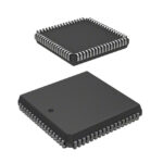 Z8S18020VEG
The activity of extra discounts on wholesale prices is in full swing…
Please fill in your contact information and we will send you the latest wholesale price list.






