 ChipApex | Global Electronic Components Supplier
SEARCH
Search Product
Search Post
— IC芯片 | 连接器 | 传感器 | 被动器件 —
Search productSearch post
— IC芯片 | 连接器 | 传感器 | 被动器件 —
Consult the customer manager about the wholesale price.
consultation hotline:86-132-6715-2157
email:[email protected]
Contact the product manager for consultation. One-stop consultation is available.
Do you want a lower wholesale price? Please send us your inquiry and we will reply immediately.
The ZL30156GGG2 is a dual-channel universal clock-rate translator manufactured by Microchip Technology (formerly Zarlink). It integrates two independent digital phase-locked loops and precision synthesizers to generate programmable clocks from 1 kHz to 720 MHz. The device features four configurable reference inputs and eight outputs, including four LVPECL and four LVCMOS drivers. It supports automatic hitless reference switching, digital holdover, and flexible rate conversion for arbitrary data rates, line coding, and FEC. The component operates within a temperature range of -40°C to +85°C and is housed in a 100-pin CABGA package.
Verify the ordering suffix GGG2 indicates lead-free construction with Tin/Silver/Copper finish. Confirm the package type is 100 Pin CABGA. Ensure compatibility with the specified operating temperature range of -40°C to +85°C. Cross-reference the manufacturer designation between Zarlink Semiconductor and Microchip Technology for accurate sourcing.
Select this component when dual-channel frequency translation is required for high-speed serial interfaces. The device supports input frequencies up to 720 MHz on differential lines and 177.5 MHz on single-ended lines. Configuration is managed via SPI or I2C interfaces. Ensure the design accommodates external loop filter components for the analog PLL sections if utilized alongside the digital PLLs.
This part belongs to the ZL30156 family of universal clock-rate translators originally developed by Zarlink Semiconductor. Following corporate acquisitions, production and documentation are maintained under Microchip Technology. The GGG2 suffix specifically denotes the commercial grade, lead-free variant of the standard ZL30156GGG model.
Publicly confirmed substitute part numbers are not available in the provided source material. Engineering changes may require verification of register compatibility and pinout alignment with existing designs.
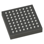 ZL30156GGG2
The activity of extra discounts on wholesale prices is in full swing…
Please fill in your contact information and we will send you the latest wholesale price list.





