 ChipApex | Global Electronic Components Supplier
SEARCH
Search Product
Search Post
— IC芯片 | 连接器 | 传感器 | 被动器件 —
Search productSearch post
— IC芯片 | 连接器 | 传感器 | 被动器件 —
Consult the customer manager about the wholesale price.
consultation hotline:86-132-6715-2157
email:[email protected]
Contact the product manager for consultation. One-stop consultation is available.
Do you want a lower wholesale price? Please send us your inquiry and we will reply immediately.
The ZL30162GDG2 is an application-specific clock and timing integrated circuit manufactured by Microchip Technology. It operates within a supply voltage range of 3V to 3.6V and supports a maximum frequency of 750MHz. The device provides one output channel and utilizes a Phase-Locked Loop (PLL) for signal synchronization. It is housed in a 144-LBGA package with dimensions of 13x13mm, designed for surface mount installation. The component functions across an industrial temperature range from -40°C to +85°C.
Verify the exact package marking and date code against the manufacturer's latest datasheet before procurement. Ensure that the 144-LBGA footprint matches the design specifications. Confirm RoHS compliance status through official documentation. Check for any recent product change notifications or lifecycle updates directly from Microchip Technology to ensure long-term availability and support.
Select this component when a single-channel, high-frequency clock solution is required for synchronous networking standards. Consider the LBGA-144 package constraints for PCB layout. Evaluate thermal performance within the specified operating temperature range. Compare against other family members if multiple outputs or different form factors are needed for the system architecture.
This part belongs to Microchip's portfolio of application-specific clock generators and timing solutions. These devices are engineered to meet the stringent jitter and phase noise requirements of modern digital communication systems. The ZL30162 series complements other timing products by providing dedicated synchronization capabilities for critical infrastructure components.
Publicly documented substitutes include ZL30163GDG2. Verify pin compatibility and electrical specifications before substitution.
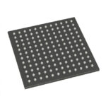 ZL30162GDG2
The activity of extra discounts on wholesale prices is in full swing…
Please fill in your contact information and we will send you the latest wholesale price list.






