 ChipApex | Global Electronic Components Supplier
SEARCH
Search Product
Search Post
— IC芯片 | 连接器 | 传感器 | 被动器件 —
Search productSearch post
— IC芯片 | 连接器 | 传感器 | 被动器件 —
Consult the customer manager about the wholesale price.
consultation hotline:86-132-6715-2157
email:[email protected]
Contact the product manager for consultation. One-stop consultation is available.
Do you want a lower wholesale price? Please send us your inquiry and we will reply immediately.
The ZL30166GDG2 is a triple-channel clock translator manufactured by Microchip Technology. It operates within a supply voltage range of 3.135 V to 3.465 V and supports input frequencies up to 750 MHz with a single output configuration. The device is housed in a 144-lead LBGA package measuring 13x13 mm. It functions reliably across an industrial temperature range from -40°C to +85°C. The component utilizes CC Plus ROM technology for configuration storage and is designed for high-performance timing applications requiring precise frequency translation.
Verify the specific suffix GDG2 against official Microchip documentation to confirm pinout, package dimensions, and electrical characteristics match system requirements. Ensure environmental compliance data aligns with project constraints. Confirm that the LBGA-144 footprint matches PCB layout specifications before finalizing procurement orders.
Select this component when triple-clock translation is required for Ethernet, Fibre Channel, or SONET/SDH applications. The 750 MHz input capability suits high-speed serial interfaces. The LBGA-144 package offers dense integration for space-constrained designs. Verify thermal performance within the -40°C to +85°C range for the intended operating environment.
This part belongs to the ZL30166 family of clock translators from Microchip Technology. It is designed for application-specific timing needs in telecommunications and data communications. The series typically includes variants with different package options and channel configurations to support diverse system architectures.
Consult official Microchip substitution guides for verified alternatives. Cross-reference pinouts and electrical parameters carefully when considering equivalent parts from other manufacturers.
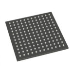 ZL30166GDG2
The activity of extra discounts on wholesale prices is in full swing…
Please fill in your contact information and we will send you the latest wholesale price list.





