 ChipApex | Global Electronic Components Supplier
SEARCH
Search Product
Search Post
— IC芯片 | 连接器 | 传感器 | 被动器件 —
Search productSearch post
— IC芯片 | 连接器 | 传感器 | 被动器件 —
Consult the customer manager about the wholesale price.
consultation hotline:86-132-6715-2157
email:[email protected]
Contact the product manager for consultation. One-stop consultation is available.
Do you want a lower wholesale price? Please send us your inquiry and we will reply immediately.
The ZL30182LFG7 is a dual-channel any-to-any clock translator manufactured by Microchip Technology. It operates within an industrial temperature range of -40°C to +85°C and utilizes a 64-LGA (10x5) surface-mount package. The device supports a maximum output frequency of 1.035 GHz and accepts input frequencies up to 1.25 GHz. It provides six outputs with selectable formats including CML, CMOS, HCSL, HSTL, LVDS, LVPECL, and SSTL. Each channel features three inputs: two differential/CMOS and one CMOS, allowing flexible clock signal translation for high-speed digital systems.
Verify the specific suffix against official documentation, as the provided reference data primarily details the ZL30182LFF7 variant. Confirm package dimensions and electrical specifications match the LFG7 designation before integration. Ensure supply chain sources provide authentic Microchip Technology components to guarantee reliability in critical timing applications.
Select this component when designing systems requiring precise frequency translation between disparate clock domains. The dual-channel architecture allows independent configuration for different interface standards. Verify that the required output voltage levels and drive strengths align with the available CML, LVDS, or CMOS options specified in the datasheet.
This device belongs to the ZL30182 family of clock translators designed for complex timing architectures. It serves as a bridge between various clock sources and destination devices, enabling system synchronization across mixed-frequency environments without requiring multiple discrete oscillators.
Direct pin-compatible replacements are not explicitly documented in the provided source material. Evaluate other members of the ZL30182 series or Microchip's broader clock generator portfolio for functional equivalence, ensuring input/output counts and frequency ranges meet design requirements.
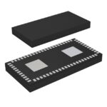 ZL30182LFG7
The activity of extra discounts on wholesale prices is in full swing…
Please fill in your contact information and we will send you the latest wholesale price list.





