 ChipApex | Global Electronic Components Supplier
SEARCH
Search Product
Search Post
— IC芯片 | 连接器 | 传感器 | 被动器件 —
Search productSearch post
— IC芯片 | 连接器 | 传感器 | 被动器件 —
Consult the customer manager about the wholesale price.
consultation hotline:86-132-6715-2157
email:[email protected]
Contact the product manager for consultation. One-stop consultation is available.
Do you want a lower wholesale price? Please send us your inquiry and we will reply immediately.
The ZL30241LDG1 is a single-channel precision universal clock generator and Numerical Control Oscillator (NCO) manufactured by Microchip Technology. It integrates one Phase-Locked Loop (PLL) capable of integer, fractional, and ratio modes to synthesize two independent output frequencies ranging from 12 MHz to 914 MHz. The device supports input references including crystals (22–54 MHz), crystal oscillators, or differential/single-ended signals up to 864 MHz. Outputs are configurable for LVDS, LVPECL, HCSL, or LVCMOS formats. Key electrical specifications include an RMS jitter of up to 275 fs in integer mode and 400 fs in fractional mode, with NCO accuracy below 0.1 ppb. It operates within a temperature range of -40°C to +85°C and is housed in a 48-pin QFN package measuring 7x7 mm.
Verify the ordering suffix against the specific packaging requirement. The ZL30241LDG1 variant is supplied in a 48-pin QFN tray. Confirm that the application design accommodates the specified operating voltage ranges and thermal characteristics for the QFN-48 package before finalizing procurement.
Select this component when a single PLL with dual independent outputs is required for high-frequency synthesis up to 914 MHz. Ensure the input reference source meets the phase noise requirements, as the PLL tracks reference noise below the loop bandwidth. Verify that the target output format (LVDS/LVPECL/HCSL/LVCMOS) aligns with the load requirements and that the system can support the necessary SPI interface for configuration.
The ZL30241 belongs to the ZL302xx series of precision clock generators. It is designed to replace discrete clock generation solutions by integrating the PLL, VCO, and output buffers into a single chip. The device supports factory-programmed defaults, allowing it to generate correct clock signals immediately at power-up without external microcontroller intervention.
Public confirmed substitute part numbers are not available in the provided documentation. Evaluate compatibility based on pinout, voltage levels, and jitter specifications if considering alternative single-PLL clock generators.
The device accepts fundamental crystals (22–54 MHz), crystal oscillators (22–180 MHz), or external reference signals (single-ended or differential, up to 864 MHz).
Ratio mode enables frequency translation of the form N + X/Y, which is ideal for FEC rate translation applications like SONET and OTN. It uses a feedback divider structure defined by parameters A, B, C, and D.
Yes, each output buffer can be independently configured via SPI registers to support LVDS, LVPECL, HCSL, or LVCMOS formats after power-up.
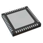 ZL30241LDG1
The activity of extra discounts on wholesale prices is in full swing…
Please fill in your contact information and we will send you the latest wholesale price list.





