 ChipApex | Global Electronic Components Supplier
SEARCH
Search Product
Search Post
— IC芯片 | 连接器 | 传感器 | 被动器件 —
Search productSearch post
— IC芯片 | 连接器 | 传感器 | 被动器件 —
Consult the customer manager about the wholesale price.
consultation hotline:86-132-6715-2157
email:[email protected]
Contact the product manager for consultation. One-stop consultation is available.
Do you want a lower wholesale price? Please send us your inquiry and we will reply immediately.
The ZL30270LDG1S is a clock generator featuring five output frequency synthesizers in a 48-lead 7 mm x 7 mm VQFN package. It supports any-to-any frequency conversion with outputs ranging from 0.5 Hz to 750 MHz. The device accepts crystal or CMOS inputs and provides up to six differential or twelve single-ended outputs. Key electrical parameters include core supply voltages of 1.8V and 3.3V, and output voltage levels between 1.5V and 3.3V. It achieves typical output jitter of 100 fsRMS at 156.25 MHz.
Verify the specific suffix 'LDG1S' against the manufacturer's official documentation to confirm exact ordering details. Confirm that the 48-lead VQFN package matches the target PCB footprint requirements. Ensure the host interface configuration aligns with the available SPI or I2C options.
Select this component when five distinct output frequencies are required from a single device. The ZL30270 variant is appropriate for designs needing up to six differential or twelve single-ended outputs. Consider the ZL30271 if ten differential or twenty single-ended outputs are necessary.
This part belongs to the ZL30270-ZL30271 family of 6- or 10-output clock generators. The ZL30270 specifically utilizes a 48-lead VQFN package, whereas the ZL30271 uses a 64-lead VQFN package. Both share identical internal synthesizer architectures and feature sets.
Public confirmed substitute part numbers are not available in the provided documentation.
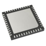 ZL30270LDG1S
The activity of extra discounts on wholesale prices is in full swing…
Please fill in your contact information and we will send you the latest wholesale price list.






