 ChipApex | Global Electronic Components Supplier
SEARCH
Search Product
Search Post
— IC芯片 | 连接器 | 传感器 | 被动器件 —
Search productSearch post
— IC芯片 | 连接器 | 传感器 | 被动器件 —
Consult the customer manager about the wholesale price.
consultation hotline:86-132-6715-2157
email:[email protected]
Contact the product manager for consultation. One-stop consultation is available.
Do you want a lower wholesale price? Please send us your inquiry and we will reply immediately.
The ZL30272LDG1S is a single-channel jitter attenuator and clock synthesizer from Microchip Technology, housed in a 48-lead 7 mm x 7 mm VQFN package. It supports up to six differential or CMOS inputs and provides up to six differential or twelve CMOS outputs. The device accepts input frequencies ranging from 1 kHz to 1250 MHz and generates output frequencies from 0.5 Hz to 750 MHz. It features a typical output jitter of 100 fsRMS at 156.25 MHz (12 kHz to 20 MHz bandwidth). Operating voltages are 1.8 V and 3.3 V, with an operating temperature range of -40°C to +85°C.
Verify the specific suffix 'S' against official documentation to confirm packaging details, as standard listings may indicate tray packaging while the suffix implies reel packaging. Confirm availability status through authorized distributors, as stock levels vary by region. Ensure the component meets RoHS compliance requirements for the target application.
Select the ZL30272LDG1S when a single-channel solution with up to six differential inputs is required. This model is suitable for applications needing up to six differential or twelve CMOS outputs. Consider the ZL30273 or ZL30274 if two independent channels or higher output counts are necessary. Verify that the 48-lead VQFN package fits the PCB layout constraints.
The ZL30272 is part of the ZL3027x family of jitter attenuators, which also includes the ZL30273 and ZL30274. These devices share similar core architectures but differ in channel count and I/O capacity. The ZL30272 specifically offers one DPLL and fewer I/O pins compared to its counterparts, making it a cost-effective option for simpler clocking topologies.
The ZL30273LDG1S and ZL30274LDG1S are pin-compatible upgrades offering additional channels and outputs. Direct replacement requires verifying that the increased I/O capacity does not conflict with existing board routing. No other cross-model substitutes are publicly confirmed.
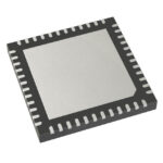 ZL30272LDG1S
The activity of extra discounts on wholesale prices is in full swing…
Please fill in your contact information and we will send you the latest wholesale price list.






