 ChipApex | Global Electronic Components Supplier
SEARCH
Search Product
Search Post
— IC芯片 | 连接器 | 传感器 | 被动器件 —
Search productSearch post
— IC芯片 | 连接器 | 传感器 | 被动器件 —
Consult the customer manager about the wholesale price.
consultation hotline:86-132-6715-2157
email:[email protected]
Contact the product manager for consultation. One-stop consultation is available.
Do you want a lower wholesale price? Please send us your inquiry and we will reply immediately.
The ZL30682LFG7 is a dual-channel, 10-input, 18-output line card timing IC designed for carrier-grade synchronization. It integrates two digital phase-locked loops (DPLLs), five output frequency families, and supports up to 10 differential or CMOS inputs ranging from 1kHz to 900MHz. The device generates output clocks from <1Hz to 1045MHz with high-resolution fractional conversion and sub-picosecond jitter. Key features include hitless reference switching, programmable bandwidth (14Hz–470Hz), and per-DPLL/input/output phase adjustment at 1ps resolution. It operates within a -40°C to +85°C temperature range in an 80-lead LGA package.
Verify the specific ordering suffix against official Microchip documentation to confirm package type and tray quantity. Confirm RoHS compliance status through the manufacturer's product compliance page before procurement. Ensure the supply chain source provides valid traceability for this component.
Select the ZL30682LFG7 when two independent DPLL channels are required for redundancy or distinct timing domains. This model accommodates up to 10 input references and provides 18 total outputs, making it suitable for complex line card architectures requiring extensive clock distribution and precise phase alignment.
This component belongs to the ZL3068x family of line card timing ICs, which includes the single-channel ZL30681 and triple-channel ZL30683 variants. All models share identical input/output counts and core timing features, differing only in the number of integrated DPLL channels available for system synchronization.
The ZL30681LFG7 serves as a single-channel alternative, while the ZL30683LFG7 provides three DPLL channels. Both share the same 80-lead LGA package and pinout compatibility.
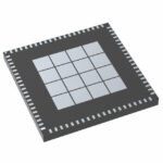 ZL30682LFG7
The activity of extra discounts on wholesale prices is in full swing…
Please fill in your contact information and we will send you the latest wholesale price list.






