 ChipApex | Global Electronic Components Supplier
SEARCH
Search Product
Search Post
— IC芯片 | 连接器 | 传感器 | 被动器件 —
Search productSearch post
— IC芯片 | 连接器 | 传感器 | 被动器件 —
Consult the customer manager about the wholesale price.
consultation hotline:86-132-6715-2157
email:[email protected]
Contact the product manager for consultation. One-stop consultation is available.
Do you want a lower wholesale price? Please send us your inquiry and we will reply immediately.
The ZL40206LDG1 is a clock buffer and fanout driver manufactured by Microchip Technology. It provides one input to eight outputs (1:8) with LVPECL output signaling. The device supports maximum input frequencies up to 750 MHz and features a typical propagation delay of 2 ns. It operates within a supply voltage range of 2.375 V to 3.465 V. The component is housed in a 32-VFQFN package with an exposed pad, suitable for surface mount installation. It functions reliably across an industrial temperature range from -40°C to +85°C.
Verify the specific suffix 'LDG1' against official Microchip documentation to confirm package type and environmental compliance. Ensure the design accommodates the 32-VFQFN exposed pad thermal requirements. Confirm that the LVPECL output levels match the receiving circuit's input specifications. Check moisture sensitivity level handling procedures during assembly. Validate that the operating temperature range meets the application's environmental constraints.
Select this component when a single clock source needs to drive multiple loads with minimal skew. The 1:8 ratio is suitable for distributing reference clocks to several synchronous components. Consider the LVPECL output format for compatibility with existing high-speed interfaces. Evaluate the 750 MHz frequency limit against the system's timing requirements. Assess the power consumption benefits compared to other buffer families.
This part belongs to the ZL4020x series of clock buffers and drivers from Microchip Technology. These devices are designed for high-performance clock distribution in complex digital systems. The series offers various fanout ratios to accommodate different system architectures. The ZL40206LDG1 specifically addresses applications requiring eight buffered outputs from a single input signal.
Public confirmed substitute part numbers are not available in the provided documentation.
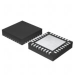 ZL40206LDG1
The activity of extra discounts on wholesale prices is in full swing…
Please fill in your contact information and we will send you the latest wholesale price list.




