 ChipApex | Global Electronic Components Supplier
SEARCH
Search Product
Search Post
— IC芯片 | 连接器 | 传感器 | 被动器件 —
Search productSearch post
— IC芯片 | 连接器 | 传感器 | 被动器件 —
Consult the customer manager about the wholesale price.
consultation hotline:86-132-6715-2157
email:[email protected]
Contact the product manager for consultation. One-stop consultation is available.
Do you want a lower wholesale price? Please send us your inquiry and we will reply immediately.
The ZL40211LDG1 is a clock fanout buffer manufactured by Microchip Technology, housed in a 32-VFQFN exposed pad package. It operates with a supply voltage range of 2.375 V to 3.465 V and supports a maximum frequency of 750 MHz. The device functions as a 2:8 multiplexer, accepting inputs from CML, HCSL, LVCMOS, LVDS, or LVPECL sources and providing eight LVPECL outputs. It is designed for surface mount installation within an operating temperature range of -40°C to +85°C.
Verify the specific suffix 'LDG1' against the manufacturer's current datasheet to confirm pinout compatibility and electrical specifications. Ensure that the required external termination components are included in the bill of materials, as the device relies on them for proper LVPECL operation. Confirm RoHS compliance status directly with the supplier documentation prior to finalizing procurement orders.
Select this component when a system requires converting various differential or single-ended clock signals into eight matched LVPECL outputs. The 2:8 multiplexer architecture allows flexibility in source selection. Consider the 32-QFN package constraints for PCB layout and thermal management. Verify that the input signal levels align with the supported standards before implementation.
This part belongs to the ZL4021x series of clock buffers from Microchip Technology. These devices are engineered for low skew and jitter performance in high-frequency applications. The ZL40211 variant specifically addresses scenarios needing multi-standard input compatibility and extensive fan-out capability within a compact footprint.
Publicly confirmed substitute part numbers are not available in the provided reference data. Consult official Microchip documentation for potential cross-reference options.
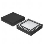 ZL40211LDG1
The activity of extra discounts on wholesale prices is in full swing…
Please fill in your contact information and we will send you the latest wholesale price list.




