 ChipApex | Global Electronic Components Supplier
SEARCH
Search Product
Search Post
— IC芯片 | 连接器 | 传感器 | 被动器件 —
Search productSearch post
— IC芯片 | 连接器 | 传感器 | 被动器件 —
Consult the customer manager about the wholesale price.
consultation hotline:86-132-6715-2157
email:[email protected]
Contact the product manager for consultation. One-stop consultation is available.
Do you want a lower wholesale price? Please send us your inquiry and we will reply immediately.
The ZL40226LDG1 is a clock fanout buffer and multiplexer IC manufactured by Microchip Technology. It accepts two differential or single-ended inputs, supporting LVPECL, LVDS, CML, HCSL, and LVCMOS logic levels. The device provides eight precision LVDS outputs. It operates at maximum input frequencies up to 750 MHz with a supply voltage range of 2.375 V to 3.465 V. The component is housed in a 32-pin VFQFN exposed pad package and functions within a temperature range of -40°C to +85°C.
Verify the specific suffix and package variant against official Microchip documentation to ensure compatibility with design requirements. Confirm that the 32-pin VFQFN footprint matches the PCB layout specifications. Check moisture sensitivity levels and reflow soldering profiles prior to assembly. Ensure input signal integrity meets the specified logic level thresholds for reliable operation across the designated temperature range.
Select this component when a system requires converting various input formats into LVDS outputs for high-speed transmission. Consider the 750 MHz frequency limit and the 2-to-8 configuration relative to system bandwidth needs. Evaluate the thermal performance within the -40°C to +85°C operating window. Compare against other buffers if different output types or pin counts are required for the specific application topology.
This part belongs to the ZL402xx series of clock timing devices from Microchip Technology. These components are designed for robust signal conditioning and distribution in complex electronic systems. The series typically includes variants with different input/output ratios and logic families, serving as critical nodes in synchronization architectures.
Consult official cross-reference data for direct substitutes. Verify that any alternative maintains the 32-pin VFQFN package and LVDS output characteristics. Ensure functional equivalence regarding input logic support and maximum frequency capabilities before implementation.
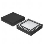 ZL40226LDG1
The activity of extra discounts on wholesale prices is in full swing…
Please fill in your contact information and we will send you the latest wholesale price list.





