 ChipApex | Global Electronic Components Supplier
SEARCH
Search Product
Search Post
— IC芯片 | 连接器 | 传感器 | 被动器件 —
Search productSearch post
— IC芯片 | 连接器 | 传感器 | 被动器件 —
Consult the customer manager about the wholesale price.
consultation hotline:86-132-6715-2157
email:[email protected]
Contact the product manager for consultation. One-stop consultation is available.
Do you want a lower wholesale price? Please send us your inquiry and we will reply immediately.
The ZL40241LDF1 is a ten-output LVCMOS fanout buffer manufactured by Microchip Technology. It operates with input frequencies up to 200 MHz and supports multiple input types including CML, HCSL, LVCMOS, LVDS, LVPECL, and SSTL. The device functions within a supply voltage range of 1.35 V to 3.465 V. It is housed in a VQFN-32 package and is rated for an operating temperature range from -40°C to +85°C.
Verify the specific suffix LDF1 corresponds to the cut-tape or reel packaging configuration required for assembly. Confirm that the VQFN-32 package dimensions align with the PCB footprint design. Ensure the input signal levels match one of the supported standards (CML, HCSL, LVCMOS, LVDS, LVPECL, SSTL) to guarantee proper operation within the specified 200 MHz limit.
Select this component when a single clock source must drive ten LVCMOS destinations. It serves as an interface between various differential input formats and standard CMOS logic. Consider the 1.35 V minimum supply voltage if the system operates at lower power rails compared to standard 3.3 V designs. The 200 MHz maximum frequency limits its use in high-speed PCIe or Ethernet applications requiring higher jitter performance or faster speeds.
This part belongs to the ZL40241 series of clock buffers. It is distinct from other ZL402x family members which may offer different output counts, such as the six-output ZL40251, or different technologies like the four-output LVDS ZL40215. The ZL40241 specifically targets applications needing ten LVCMOS outputs.
Direct replacements within the same manufacturer line include variants with different packaging options, such as tray-packaged versions if available. Cross-manufacturer equivalents would require matching the ten-output LVCMOS specification, 200 MHz frequency, and compatible input voltage ranges.
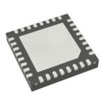 ZL40241LDF1
The activity of extra discounts on wholesale prices is in full swing…
Please fill in your contact information and we will send you the latest wholesale price list.




