 ChipApex | Global Electronic Components Supplier
SEARCH
Search Product
Search Post
— IC芯片 | 连接器 | 传感器 | 被动器件 —
Search productSearch post
— IC芯片 | 连接器 | 传感器 | 被动器件 —
Consult the customer manager about the wholesale price.
consultation hotline:86-132-6715-2157
email:[email protected]
Contact the product manager for consultation. One-stop consultation is available.
Do you want a lower wholesale price? Please send us your inquiry and we will reply immediately.
The ZL40262LDF1 is a two-output ultra-low additive jitter fanout buffer manufactured by Microchip Technology. It accepts one differential input and provides two differential HCSL outputs, supporting clock frequencies from 0 MHz to 400 MHz. The device operates on 2.5V or 3.3V power supplies and features an embedded low-drop-out (LDO) voltage regulator for superior power supply noise rejection. Key electrical specifications include an additive jitter of 32 fs in the 12 kHz to 20 MHz integration band at 400 MHz, a maximum output-to-output skew of 50 ps, and individual output enable pins for each differential pair.
Verify the specific ordering suffix 'LDF1' against the manufacturer's current product identification system to confirm package type and tape-and-reel configuration. Ensure that the required power supply voltages (2.5V or 3.3V) match the design specifications, as both VDD and VDDO must be connected to the same voltage level during operation.
Select this component when ultra-low phase noise is critical for high-speed serial interfaces like PCIe Gen 5 or UPI. The device supports input frequencies up to 400 MHz and offers flexible termination options for HCSL outputs. Consider the 4 mm x 4 mm VQFN package dimensions and thermal properties if space constraints are a primary design factor.
The ZL40262 belongs to Microchip's family of ultra-low additive jitter fanout buffers designed for high-performance computing and communication applications. It complements other devices in the series by providing a compact solution for distributing reference clocks with minimal added noise, specifically targeting next-generation interface standards requiring stringent jitter budgets.
Publicly confirmed substitute part numbers are not available in the provided documentation. Verify compatibility with existing designs by comparing pin configurations, electrical characteristics, and package dimensions before considering alternative components.
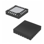 ZL40262LDF1
The activity of extra discounts on wholesale prices is in full swing…
Please fill in your contact information and we will send you the latest wholesale price list.





