 ChipApex | Global Electronic Components Supplier
SEARCH
Search Product
Search Post
— IC芯片 | 连接器 | 传感器 | 被动器件 —
Search productSearch post
— IC芯片 | 连接器 | 传感器 | 被动器件 —
Consult the customer manager about the wholesale price.
consultation hotline:86-132-6715-2157
email:[email protected]
Contact the product manager for consultation. One-stop consultation is available.
Do you want a lower wholesale price? Please send us your inquiry and we will reply immediately.
The ZL40272LDG1 is a low-skew, low additive jitter fanout buffer featuring twelve differential outputs and three inputs. It supports HCSL, LVDS, and LVPECL output formats with individual enable control. The device accepts differential or single-ended signals on two inputs and a crystal or single-ended signal on the third. It operates from 2.5V or 3.3V supplies, supporting clock frequencies up to 1.5 GHz. Additive jitter is specified at 24 fs (12 kHz to 20 MHz at 625 MHz). Maximum output-to-output skew is 50 ps. Control is via I2C or hardware pins.
Verify the datasheet revision DS20006408D against the specific manufacturing lot. Confirm the package marking matches the 56-Lead 8 mm x 8 mm QFN outline. Ensure the ordering suffix LDG1 corresponds to the tray packaging format if required by the assembly process. Check for any associated errata sheets for silicon revisions.
Select this component when low additive jitter and high output count are required. Verify that the input signal format (LVPECL, HCSL, LVDS, SSTL, CML, LVCMOS) is compatible with the programmable common mode settings. Ensure the application supports the 2.5V or 3.3V VDDO supply requirements for the selected output type.
This part belongs to the SmartBuffer family of clock distribution devices. It provides a solution for distributing reference clocks in high-speed serial interfaces. The device integrates an internal crystal oscillator circuit, reducing external component count compared to discrete solutions.
Public confirmed substitute part numbers are not available in the provided documentation.
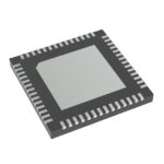 ZL40272LDG1
The activity of extra discounts on wholesale prices is in full swing…
Please fill in your contact information and we will send you the latest wholesale price list.





