 ChipApex | Global Electronic Components Supplier
SEARCH
Search Product
Search Post
— IC芯片 | 连接器 | 传感器 | 被动器件 —
Search productSearch post
— IC芯片 | 连接器 | 传感器 | 被动器件 —
Consult the customer manager about the wholesale price.
consultation hotline:86-132-6715-2157
email:[email protected]
Contact the product manager for consultation. One-stop consultation is available.
Do you want a lower wholesale price? Please send us your inquiry and we will reply immediately.
The ZL81001GGG2 is a DS1/E1/2048kHz transceiver designed for BITS and SSU timing in carrier-grade telecommunications equipment. It supports full DS1, E1, and G.703 synchronization signal handling with SSM message insertion and extraction. The device integrates two composite clock receivers compliant with Telcordia GR-378 and ITU-T standards, alongside two programmable-frequency inputs. Powered by a single 12.8MHz local oscillator, it operates at 1.8V with 3.3V I/O (5V tolerant). It features an 8-bit parallel or SPI serial processor interface and functions within the industrial temperature range of -40°C to +85°C.
Verify the specific ordering suffix GGG2 against the manufacturer's current documentation to confirm package type and tray configuration. Ensure compatibility with the required industrial temperature range (-40°C to +85°C) and voltage specifications (1.8V core, 3.3V I/O). Confirm that the 256-pin CSBGA package fits the target PCB layout constraints.
Select this component when designing systems requiring direct DS1, E1, or 2048kHz synchronization interfaces without external framer chips. It is suitable for applications needing integrated composite clock reception and flexible line interface termination. Consider the 256-pin CSBGA package size and thermal requirements during the initial hardware design phase.
The ZL81001 belongs to Microchip's family of BITS/SSU timing transceivers. This specific part number denotes the 256-pin CSBGA package variant intended for high-density carrier-grade applications. It provides comprehensive timing recovery and generation capabilities for synchronous digital hierarchy networks.
Consult official Microchip documentation for confirmed substitute part numbers. Verify pinout and register compatibility before replacing existing components in production designs.
It complies with ANSI T1.101/T1.102/T1.107, ITU-T G.703/G.704/G.706/G.775/G.823/G.824/G.825, Telcordia GR-378-CORE, and IEEE 1149.1.
The ZL81001 operates from a single 12.8MHz local oscillator connected to the REFCLK pin, with internal logic running at 1.8V and 3.3V I/O that is 5V tolerant.
It supports two composite clock receivers (IC1A/IC2A), two general-purpose CMOS clock inputs, and a BITS receiver for DS1, E1, 2048kHz, or 6312kHz signals.
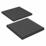 ZL81001GGG2
The activity of extra discounts on wholesale prices is in full swing…
Please fill in your contact information and we will send you the latest wholesale price list.





