 ChipApex | Global Electronic Components Supplier
SEARCH
Search Product
Search Post
— IC芯片 | 连接器 | 传感器 | 被动器件 —
Search productSearch post
— IC芯片 | 连接器 | 传感器 | 被动器件 —
Consult the customer manager about the wholesale price.
consultation hotline:86-132-6715-2157
email:[email protected]
Contact the product manager for consultation. One-stop consultation is available.
Do you want a lower wholesale price? Please send us your inquiry and we will reply immediately.
The Goford Semiconductor 06N06L is an N-channel enhancement mode power MOSFET utilizing advanced trench technology. It features a drain-source voltage (VDS) of 60V and a continuous drain current (ID) of 5.5A at 25°C case temperature. The device offers a maximum on-resistance (RDS(on)) of 45mΩ at VGS=10V and 50mΩ at VGS=4.5V. Key dynamic parameters include a gate charge (Qg) of 16nC, input capacitance (Ciss) of 765pF, and reverse transfer capacitance (Crss) of 40pF. It operates within a junction temperature range of -55°C to +150°C.
Verify the specific datasheet revision (e.g., A1514.16-V1.2) matches your design requirements. Confirm RoHS compliance status as indicated in the documentation. Ensure thermal management aligns with the specified RthJA of 62.5 ºC/W for your PCB layout. Check package marking 'L' for SOT-23-3 identification during assembly.
Select this component for applications requiring a 60V N-channel MOSFET in a compact SOT-23-3 package. Consider the 45mΩ RDS(on) at 10V drive for low conduction losses. Evaluate the 16nC gate charge against your driver capability for switching speed requirements. Verify that the 5.5A continuous current rating suits your thermal dissipation constraints.
This part belongs to the Goford Semiconductor power MOSFET portfolio, specifically designed using trench technology for improved performance over planar devices. It targets general-purpose switching applications where size and efficiency are critical. The SOT-23-3 package allows for high-density surface mount placement on printed circuit boards.
No public substitute part numbers are documented in the provided source material.
The maximum pulsed drain current (IDM) is 22A, limited by the maximum junction temperature.
Yes, it has a gate-source threshold voltage (VGS(th)) ranging from 1.0V to 2.5V, allowing operation with low gate drive voltages.
The reverse recovery time (Trr) is typically 29ns when tested at IF=5A and di/dt=100A/us.
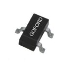 06N06L
The activity of extra discounts on wholesale prices is in full swing…
Please fill in your contact information and we will send you the latest wholesale price list.





