ChipApex | Global Electronic Components Supplier
SEARCH
Search Product
Search Post
— IC芯片 | 连接器 | 传感器 | 被动器件 —
Search productSearch post
— IC芯片 | 连接器 | 传感器 | 被动器件 —
Consult the customer manager about the wholesale price.
consultation hotline:86-132-6715-2157
email:[email protected]
Contact the product manager for consultation. One-stop consultation is available.
Do you want a lower wholesale price? Please send us your inquiry and we will reply immediately.
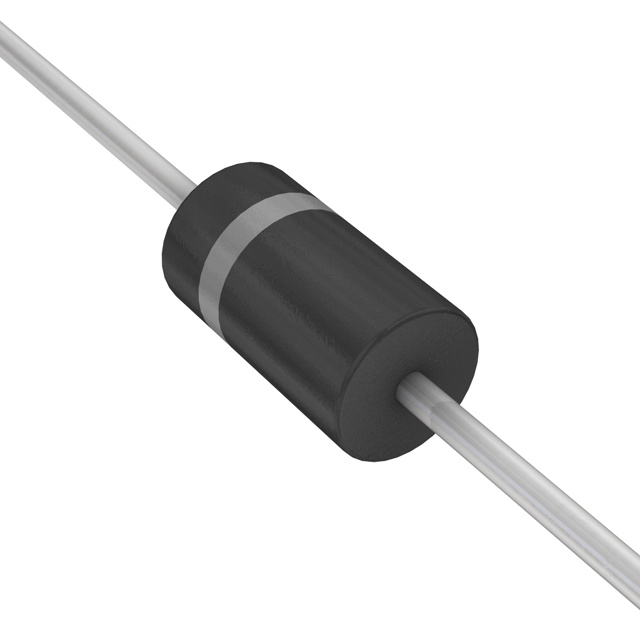
The onsemi 1N5822 is a Schottky barrier rectifier utilizing metal-to-silicon power diode technology. It features a DO-201AD axial package with two pins for through-hole installation. Key electrical parameters include a maximum repetitive peak reverse voltage (Vrrm) of 40 V and a maximum continuous forward current (If) of 3 A. The device exhibits a typical peak reverse recovery time (trr) of 1.6 ns and a maximum forward voltage (Vf) of 950 mV at rated current. It supports a peak non-repetitive forward surge current (Ifsm) of 80 A and operates within a junction temperature range from -65°C to 125°C.
Verify the specific ordering suffix when purchasing, as variations such as RL indicate tape and reel packaging while standard suffixes may denote bag packing. Confirm RoHS compliance status and lead-free availability directly with the manufacturer or authorized distributors, as these attributes depend on the specific production batch and part variant selected.
Select this component for applications requiring fast switching speeds and low forward voltage drops at moderate current levels. Ensure the circuit's peak reverse voltage does not exceed 40 V and the average forward current remains within the 3 A limit. Consider the DO-201AD package constraints for thermal management and physical space requirements in the final design.
This component belongs to the 1N5822 series of axial lead rectifiers manufactured by onsemi. The series utilizes state-of-the-art chrome barrier metal technology. It is functionally comparable to other industry-standard 3A Schottky rectifiers but is distinguished by its specific manufacturing geometry and passivation techniques designed for reliability in power conversion environments.
Cross-reference with Vishay 1N5822-E3/92 or Taiwan Semiconductor 1N5822A0 for equivalent specifications. Verify that substitute parts maintain the same 40 V rating, 3 A current capacity, and DO-201AD package dimensions to ensure mechanical and electrical compatibility without redesigning the PCB footprint.
 1N5822
The activity of extra discounts on wholesale prices is in full swing…
Please fill in your contact information and we will send you the latest wholesale price list.