 ChipApex | Global Electronic Components Supplier
SEARCH
Search Product
Search Post
— IC芯片 | 连接器 | 传感器 | 被动器件 —
Search productSearch post
— IC芯片 | 连接器 | 传感器 | 被动器件 —
Consult the customer manager about the wholesale price.
consultation hotline:86-132-6715-2157
email:[email protected]
Contact the product manager for consultation. One-stop consultation is available.
Do you want a lower wholesale price? Please send us your inquiry and we will reply immediately.
The 2304NZLPGGI is a high-performance, low skew, low jitter 1:4 LVCMOS clock buffer manufactured by Renesas Electronics Corporation. It supports a synchronous glitch-free Output Enable function to eliminate incorrect output clock cycles during enable or disable operations. The device operates on a 1.8V to 3.3V power supply and features an industrial temperature range from -40°C to +85°C. It is packaged in an 8-pin TSSOP with a 0.65mm pitch. Key electrical parameters include a maximum input frequency of 200 MHz, a typical propagation delay of 1.7 ns at 3.3V, and a maximum output-to-output skew of 40 ps.
Verify the package type matches the required PCB footprint, as the 2304NZL series is available in DFN, SOIC, and TSSOP variants. Confirm that the specific ordering suffix 'PGGI' corresponds to the 8-pin TSSOP tube packaging. Ensure the design accounts for identical trace geometries and loads on all four outputs to maintain the specified 40 ps skew performance.
Select this component when a 1:4 LVCMOS clock buffer with low skew and glitch-free enable functionality is required. The device supports input frequencies up to 200 MHz and additive phase jitter as low as 30 fs RMS at 3.3V. Consider board layout constraints, as achieving minimum skew requires identical terminations and trace lengths for all four outputs.
The 2304NZLPGGI belongs to the 2304NZL family of high-performance clock buffers. This family includes variants with different package options such as the 2304NZLDCGI (SOIC) and 2304NZLNTGI (DFN). All variants share the same core electrical specifications and functionality, differing primarily in physical package dimensions and carrier types.
Direct replacements within the same family include 2304NZLDCGI (SOIC) and 2304NZLNTGI (DFN), provided the package form factor is compatible with the existing PCB layout. Other pin-compatible alternatives should be verified against the datasheet for matching electrical characteristics and package dimensions.
The 2304NZL supports a maximum input frequency of 200 MHz.
The Output Enable (OE) pin controls the clock outputs synchronously. When OE is HIGH, the outputs are enabled. When OE is LOW, the outputs are forced to logic LOW. The function is glitch-free to prevent incorrect clock cycles during state transitions.
At a supply voltage of 3.3V, the typical propagation delay is 1.7 ns, with a maximum of 2.1 ns.
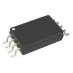 2304NZLPGGI
The activity of extra discounts on wholesale prices is in full swing…
Please fill in your contact information and we will send you the latest wholesale price list.






