 ChipApex | Global Electronic Components Supplier
SEARCH
Search Product
Search Post
— IC芯片 | 连接器 | 传感器 | 被动器件 —
Search productSearch post
— IC芯片 | 连接器 | 传感器 | 被动器件 —
Consult the customer manager about the wholesale price.
consultation hotline:86-132-6715-2157
email:[email protected]
Contact the product manager for consultation. One-stop consultation is available.
Do you want a lower wholesale price? Please send us your inquiry and we will reply immediately.
The Renesas 2305-1HDCG is a zero-delay clock buffer featuring an integrated Phase-Locked Loop (PLL). It accepts one LVCMOS input and provides five low-skew LVCMOS outputs. The device operates at frequencies from 10 MHz to 133 MHz with a supply voltage range of 3 V to 3.6 V. Key electrical parameters include a maximum propagation delay of 0 ps, cycle-to-cycle jitter under 200 ps, and output skew less than 250 ps. It utilizes a high-drive -1H variant architecture for faster rise and fall times, housed in an 8-pin SOIC package.
Verify component status as the 2305-1HDCG may be discontinued or superseded by newer revisions such as the 2305-1HDCGI8. Confirm moisture sensitivity level and lead-free compliance against current RoHS requirements before procurement. Check for available alternative packaging options like tape-and-reel if tube quantities are unavailable.
Select this part for applications requiring precise phase alignment between source and destination clocks without external RC networks. The -1H suffix indicates higher drive strength compared to standard variants. Ensure the design supports the 3.3V operating voltage and that the 8-pin SOIC footprint matches the PCB layout constraints.
This component belongs to the IDT/Renesas 2305 family of zero-delay buffers. It serves as a high-speed clock distributor designed to minimize jitter and skew in digital systems. The device integrates the PLL feedback loop internally, simplifying board design compared to discrete solutions.
The 2305-1HDCGI8 is a verified equivalent offering industrial temperature range support. Other family members like the 2305-1DCG provide similar functionality but may differ in drive strength or temperature specifications.
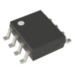 2305-1HDCG
The activity of extra discounts on wholesale prices is in full swing…
Please fill in your contact information and we will send you the latest wholesale price list.





