 ChipApex | Global Electronic Components Supplier
SEARCH
Search Product
Search Post
— IC芯片 | 连接器 | 传感器 | 被动器件 —
Search productSearch post
— IC芯片 | 连接器 | 传感器 | 被动器件 —
Consult the customer manager about the wholesale price.
consultation hotline:86-132-6715-2157
email:[email protected]
Contact the product manager for consultation. One-stop consultation is available.
Do you want a lower wholesale price? Please send us your inquiry and we will reply immediately.
The Renesas 2305-1PGG is a high-speed PLL-based clock buffer designed for zero delay applications. It operates at 3.3V and provides four low-skew outputs with speeds up to 133 MHz. The device features an on-chip PLL feedback loop, ensuring minimal propagation delay between input and output signals. It supports tri-state mode for board-level testing and offers full CMOS outputs with sufficient drive capability. The component is housed in an 8-pin TSSOP package and is suitable for industrial temperature ranges.
Verify the specific suffix requirements against the official datasheet to ensure correct package type and temperature range. Confirm that the 8-pin TSSOP form factor matches the target PCB layout constraints. Check for any RoHS compliance documentation if environmental regulations apply to the end product. Ensure the supply chain source is authorized to guarantee component authenticity and traceability.
Select this component when zero delay performance is critical for system synchronization. The 2305-1PGG variant specifically utilizes the TSSOP package, which differs from SOIC options in physical footprint. Consider the 133 MHz maximum frequency limit relative to the system clock requirements. Evaluate the need for tri-state capabilities during the design phase to determine if this feature aligns with testing strategies.
The 2305 series comprises low phase noise, high-speed PLL-based buffers. The 2305-1PGG is a specific variant within this family, distinguished by its TSSOP packaging. It shares core functionalities with other 2305 models, such as zero delay buffering and low skew outputs, but differs in physical dimensions and potentially thermal characteristics due to the package type.
The 2305-1DCG is a direct functional substitute offering identical electrical specifications but packaged in an 8-pin SOIC format. Designers must verify pinout compatibility and mechanical fit before swapping between TSSOP and SOIC packages. Other variants like the 2305-1HDCGI provide similar performance with different drive strengths or temperature ratings.
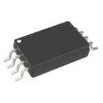 2305-1PGG
The activity of extra discounts on wholesale prices is in full swing…
Please fill in your contact information and we will send you the latest wholesale price list.





