 ChipApex | Global Electronic Components Supplier
SEARCH
Search Product
Search Post
— IC芯片 | 连接器 | 传感器 | 被动器件 —
Search productSearch post
— IC芯片 | 连接器 | 传感器 | 被动器件 —
Consult the customer manager about the wholesale price.
consultation hotline:86-132-6715-2157
email:[email protected]
Contact the product manager for consultation. One-stop consultation is available.
Do you want a lower wholesale price? Please send us your inquiry and we will reply immediately.
The Renesas 2305B-1HDCG is a zero-delay clock multiplier IC designed for high-speed clock distribution. It accepts a single reference input and drives two banks of four outputs, providing multiplication factors of 1x, 2x, or 4x depending on address pin configuration. The device utilizes an internal Phase-Locked Loop (PLL) to align output phase with the input clock, achieving zero delay. It operates at frequencies from 10 MHz to 133 MHz with a supply voltage range of 3 V to 3.6 V. Key electrical parameters include output skew less than 200 ps and cycle-to-cycle jitter under 200 ps peak-to-peak. The component is housed in an 8-pin SOIC package.
Verify the specific suffix 'CG' against official Renesas documentation to confirm the package type and temperature range. Ensure the required multiplication factor (1x, 2x, or 4x) matches the application's address pin configuration. Confirm RoHS compliance status through the manufacturer's current datasheet before procurement.
Select this part when external feedback control is needed to manage delay between the reference clock and multiplied outputs. Compare against the standard 2305 buffer if multiplication is not required. Verify that the 133 MHz maximum frequency meets system requirements. Check if the industrial temperature range (-40°C to +85°C) is necessary for the operating environment.
The 2305B series belongs to Renesas' family of high-speed PLL clock multipliers. It differs from the 2305 buffer by offering configurable multiplication ratios via address pins and an external feedback loop. This distinguishes it from fixed-ratio buffers like the 2309A, which lacks multiplication capabilities.
Direct substitutes may include other IDT/Renesas zero-delay multipliers such as the 2308B variants. Verify pin compatibility and multiplication settings. Cross-reference with generic clock multipliers only if external feedback and specific skew requirements can be met.
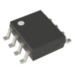 2305B-1HDCG
The activity of extra discounts on wholesale prices is in full swing…
Please fill in your contact information and we will send you the latest wholesale price list.





