 ChipApex | Global Electronic Components Supplier
SEARCH
Search Product
Search Post
— IC芯片 | 连接器 | 传感器 | 被动器件 —
Search productSearch post
— IC芯片 | 连接器 | 传感器 | 被动器件 —
Consult the customer manager about the wholesale price.
consultation hotline:86-132-6715-2157
email:[email protected]
Contact the product manager for consultation. One-stop consultation is available.
Do you want a lower wholesale price? Please send us your inquiry and we will reply immediately.
The Renesas 2305B-1PGGI8 is a high-speed phase-locked loop (PLL) clock buffer designed for zero-delay clock distribution. It operates on a single 3.3V supply voltage within the 2305 series family. The device features eight outputs with LVCMOS output types and accepts an LVCMOS input signal. It supports maximum output frequencies up to 133 MHz with a maximum propagation delay of 0 ps. The component functions within a temperature range of -40°C to +85°C and is housed in an 8-pin TSSOP package.
Verify the specific suffix '1PGGI8' against official Renesas documentation to confirm the exact package type, tape-and-reel specifications, and RoHS compliance status. Ensure the ordering information matches the current datasheet revision to avoid discrepancies in pinout or electrical characteristics during procurement.
Select this component when zero-propagation-delay performance is required for synchronous digital systems. The 3.3V operating voltage and eight-output capacity make it suitable for distributing reference clocks to multiple high-speed peripherals. Confirm that the LVCMOS input/output levels align with the source and load devices in the target circuit architecture.
This part belongs to the Renesas 2305 series of clock buffers. The series utilizes PLL technology to eliminate clock skew between input and output signals. The 2305B variant specifically targets applications requiring robust clock integrity at standard 3.3V logic levels, distinguishing it from lower-voltage or higher-frequency variants within the broader product line.
Official substitutes include IDT2305-1PGGI8 and other members of the 2305 family such as 2305-1HDCGI8, provided they match the required output count and voltage specifications.
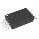 2305B-1PGGI8
The activity of extra discounts on wholesale prices is in full swing…
Please fill in your contact information and we will send you the latest wholesale price list.







