 ChipApex | Global Electronic Components Supplier
SEARCH
Search Product
Search Post
— IC芯片 | 连接器 | 传感器 | 被动器件 —
Search productSearch post
— IC芯片 | 连接器 | 传感器 | 被动器件 —
Consult the customer manager about the wholesale price.
consultation hotline:86-132-6715-2157
email:[email protected]
Contact the product manager for consultation. One-stop consultation is available.
Do you want a lower wholesale price? Please send us your inquiry and we will reply immediately.
The Renesas 2308-5HDCG is a 3.3V zero-delay clock multiplier housed in a 16-pin SOIC package. It operates within an input frequency range of 10MHz to 133MHz, utilizing LVCMOS input and output types. The device features two banks of four outputs each, with separate enable controls for each bank. Key electrical parameters include an output skew of less than 200ps and cycle-to-cycle jitter under 200ps. It supports spread spectrum input compatibility and offers external feedback pin synchronization. The component functions as a high-speed PLL clock distributor designed for precise phase alignment between input and output clocks.
Verify the specific suffix 'H' indicates high-drive capability compared to standard variants. Confirm the DC package code corresponds to the SOIC-16 form factor. Check for RoHS compliance status and moisture sensitivity level (MSL 3) requirements during storage and handling. Ensure the 3.3V core voltage matches the target system power rails.
Select this variant when high-drive strength is required for the output buffers. Compare against IDT2308-1 or -2 if lower drive or different multiplication ratios are sufficient. Verify that the 10-133MHz operating range covers the application's frequency needs. Consider the 16-SOIC package dimensions for PCB layout constraints.
This component belongs to the IDT 2308 family of zero-delay clock multipliers. It is part of the broader portfolio managed by Renesas Electronics following acquisitions. The '5H' designation typically denotes specific drive strength or configuration options within the 2308 series, distinct from the base 2308 models.
IDT2308-5HDCGI is a lead-free equivalent variant. IDT2308B-5HDCG may serve as a functional replacement within the B-series lineup. Verify pinout compatibility and electrical specifications before substitution.
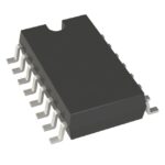 2308-5HDCG
The activity of extra discounts on wholesale prices is in full swing…
Please fill in your contact information and we will send you the latest wholesale price list.





